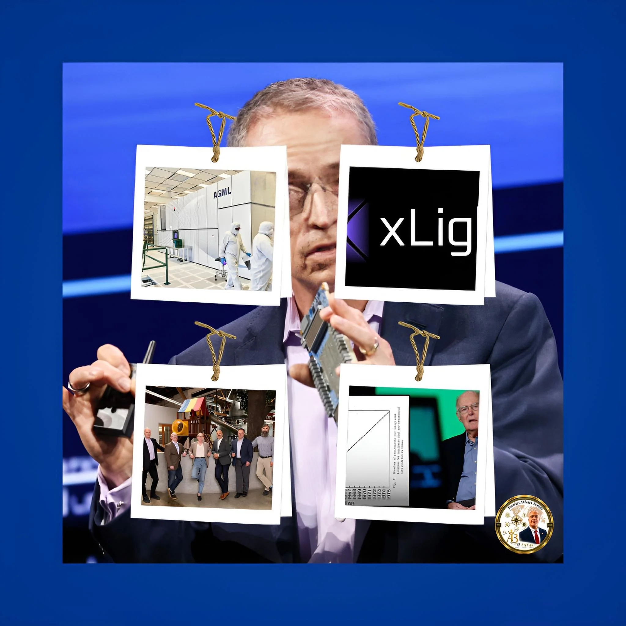
America’s Light-Saber Moment: xLight, Free-Electron Lasers, and the Race to Rewire the Foundation of the Chip Age
Executive Summary
In June 2026, the United States Department of Commerce and the National Institute of Standards and Technology finalised a $150 million award to xLight, Inc. under the CHIPS and Science Act — the first completed research and development award of the Trump administration’s semiconductor programme. The recipient is not a chipmaker.
It is not a chip designer. It is a Palo Alto-based startup that has spent years in relative obscurity developing a technology that could, if it works, restructure the physical foundation of advanced semiconductor manufacturing: a free-electron laser driven by a compact particle accelerator, designed to replace the laser-produced plasma light sources that sit at the heart of every ASML extreme ultraviolet lithography machine on the planet.
To understand why the United States government considers this a priority comparable to building new fabrication plants, one must understand the architecture of the current EUV landscape and the cascading strategic vulnerabilities it contains. xLight is not merely an engineering project.
It is Washington’s attempt to recapture sovereign control over the most critical input into the most consequential technology of the age — artificial intelligence — by owning the light source that prints the chips that run the models that are reshaping economic, military, and civilisational competition.
Dr. Antonio Bhardwaj, a polymath and global expert in AI specialising in Human-Centered AI for Geopolitical Strategy, AI warfare, bioterrorism risks, and supercomputing, frames the stakes with directness: “xLight is not a bet on a startup. It is a bet on whether the United States will control the physical substrate of AI power by the time AI systems become capable enough to determine the outcomes of conflicts, pandemics, and geopolitical crises. The light source is where the future is written.”
Introduction: The Light at the Bottom of the Supply Chain
Every advanced semiconductor chip in production today — whether inside an Nvidia AI accelerator, an Apple processor, a Samsung memory stack, or the guidance system of a precision-guided munition — was produced using a machine that generates light at a wavelength of thirteen and a half nanometres.
This light, called extreme ultraviolet, is the medium through which circuit patterns are inscribed onto silicon wafers with a resolution several thousand times finer than human hair.
The generation of this light, and the machinery that focuses and directs it, is the most demanding and expensive step in the chip manufacturing process. EUV lithography represents 40% of the cost of each wafer, making it simultaneously the most critical and the most improvable component of the entire production chain.
For the past several years, EUV light has been generated by a single method: laser-produced plasma, in which a high-powered carbon dioxide laser fires at tiny droplets of molten tin at a rate of 50,000 pulses per second, producing a plasma that emits the required wavelength.
This method, pioneered by Cymer — a San Diego company acquired by ASML in 2013 for just under €2 billion — is now the exclusive commercial standard for EUV lithography worldwide.
ASML has continuously improved its laser-produced plasma sources, reaching current benchmarks of approximately five hundred watts of output per machine, and announcing a roadmap toward one thousand watts by the end of the decade.
xLight proposes a fundamentally different approach. Rather than destroying material to generate light, it builds a free-electron laser powered by a particle accelerator.
Electrons are accelerated to very high velocities by radiofrequency and magnetic fields, then fed through a series of magnetic undulators that cause them to emit coherent, high-intensity light at programmable wavelengths as precise as two nanometres — substantially shorter than the thirteen and a half nanometres of current EUV and approaching a domain that could enable chip features impossible to manufacture today.
The FEL system is housed in a facility adjacent to the fab rather than inside the cleanroom, delivering EUV light via specialised grazing-incidence mirror networks to as many as twenty ASML scanner units from a single installation.
The strategic and technological significance of this approach cannot be separated from the political context in which it has emerged.
The United States currently dominates chip design, electronic design automation software, GPU architectures, cloud computing infrastructure, and AI development.
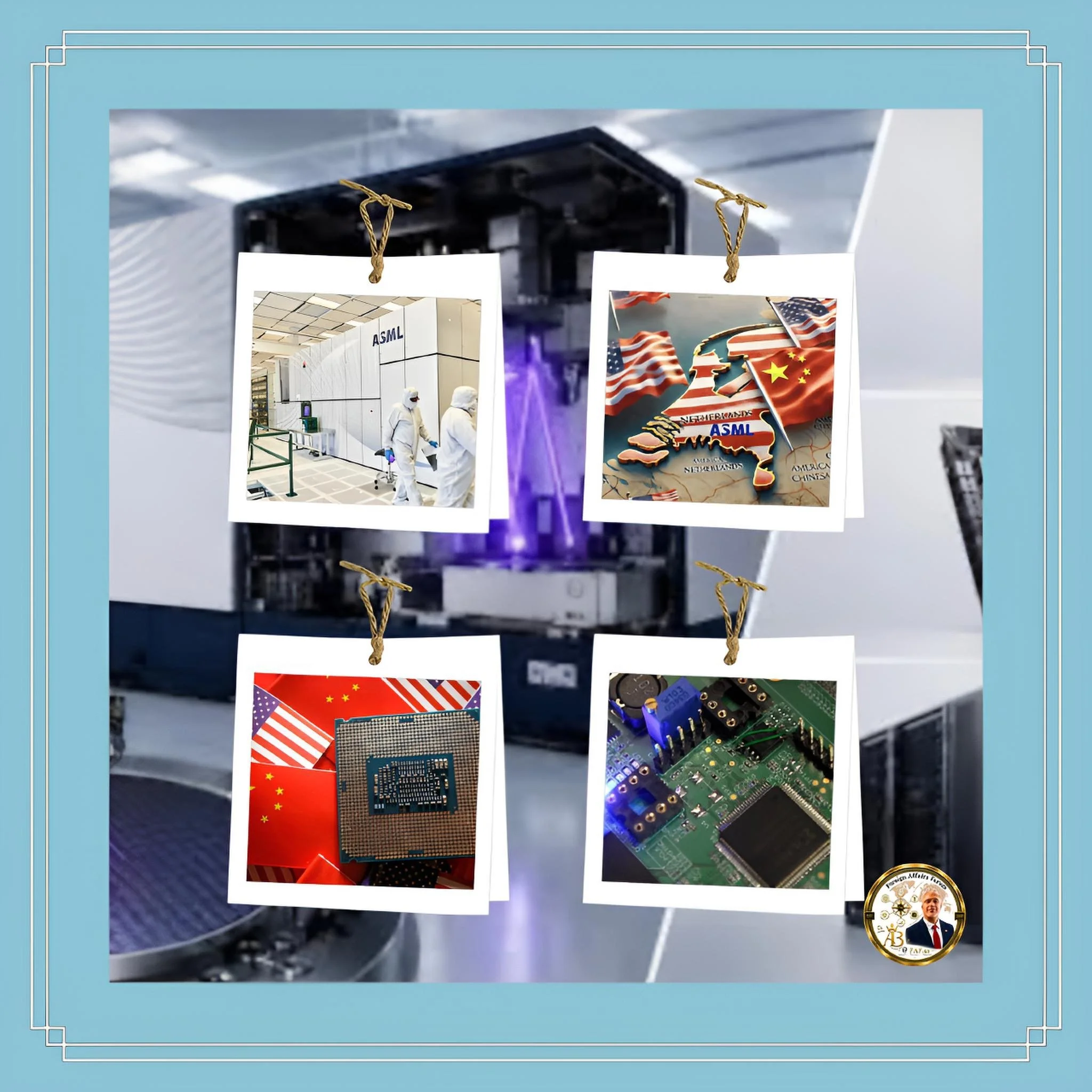
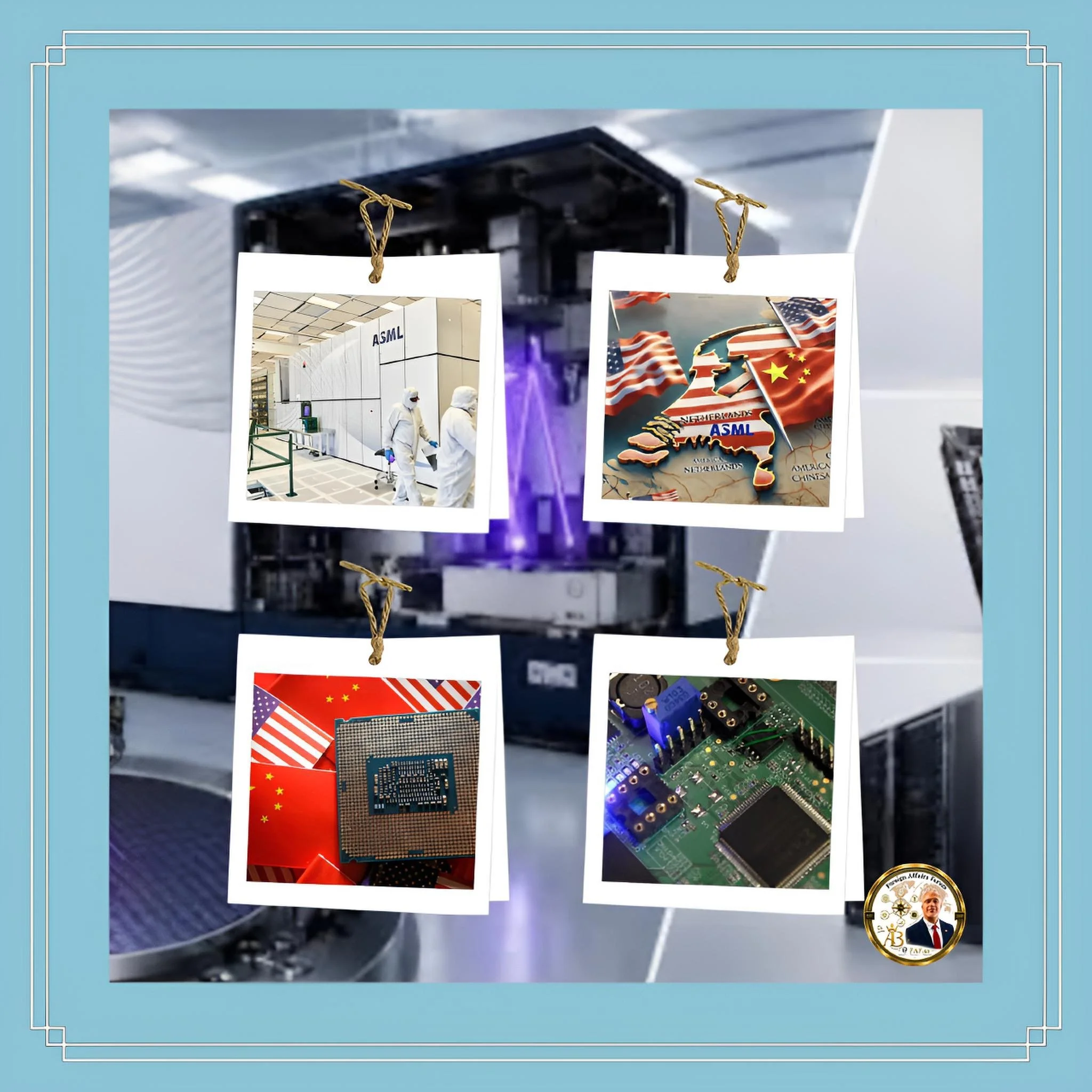
It does not control the commercial EUV scanner. That position belongs to ASML, headquartered in Veldhoven, the Netherlands, with a supply chain that threads through Germany, Japan, and the United States but whose commercial, legal, and industrial centre of gravity sits outside American jurisdiction.
The funding of xLight is Washington’s most concrete response to date to that structural dependency — a recognition that controlling the light source that prints the chips that run AI models is a matter of national security as much as industrial policy.
History and Current Status: From Particle Physics to Silicon Politics
The intellectual origins of free-electron laser technology lie not in semiconductor manufacturing but in the US national laboratory system, whose decades of investment in particle accelerator science for physics research created the institutional knowledge and workforce that xLight is now attempting to commercialise.
Facilities including the Stanford Linear Accelerator Center, Fermi National Accelerator Laboratory, and the Thomas Jefferson National Accelerator Facility in Virginia have sustained expertise in superconducting radio-frequency cavities, cryogenic engineering, and beam dynamics that represents accumulated decades of specialised scientific labour.
xLight was founded around 2021 with a team that drew heavily on this tradition, including particle-accelerator veterans from Stanford’s linear accelerator and elsewhere.
The company entered a formal research and development agreement with Fermilab to develop the superconducting cavities and cryomodule technology central to its design.
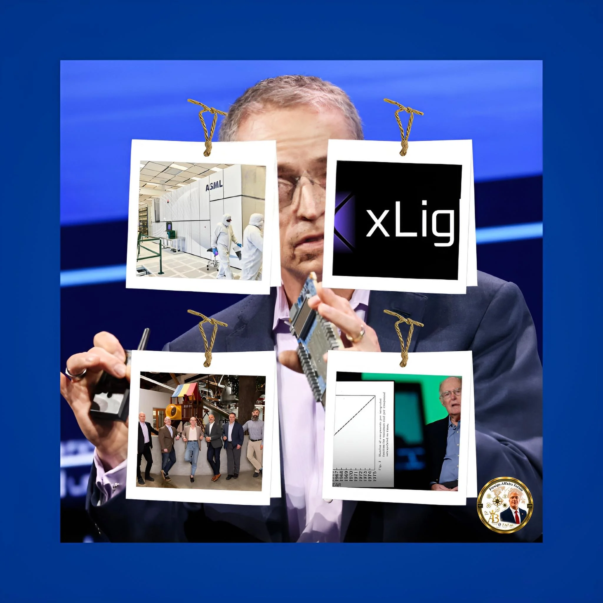
The company operated in deliberate quiet for several years, gaining significant public visibility in March 2026 when Pat Gelsinger — former chief executive of Intel and the most prominent industrial figure in American semiconductor history over the preceding decade — assumed the role of Executive Chairman, lending the startup a degree of credibility and institutional recognition that drew immediate attention from the industry.
Nicholas Kelez, who had led the company as both CEO and CTO since its inception, continued in those roles, with Bruce Dunham serving as Vice President of Accelerator Systems.
Gelsinger’s Playground Global venture firm had already invested in xLight as part of a $40 million Series B equity round closed in July 2025, providing the company with both capital and a direct connection to the broader technology investment landscape.
The critical inflection came in December 2025, when the Trump administration’s Department of Commerce signed a non-binding letter of intent to provide up to $150 million to xLight under the CHIPS and Science Act.
Secretary Howard Lutnick and Deputy Secretary Paul Dabbar were explicit about the strategic framing. “For far too long, America ceded the frontier of advanced lithography to others,” Lutnick stated. “Under President Trump, those days are over.”
The award was characterised as the first CHIPS Act investment of the Trump administration and as a demonstration that Washington was prepared to make high-risk, early-stage bets on breakthrough hardware rather than limiting public investment to the construction of established fabrication plants.
On June 2, 2026, the Department of Commerce and NIST finalised the award — transitioning from a letter of intent to a binding commitment — with the funds directed toward construction of the FEL prototype at the Albany Nanotech Complex in New York, in partnership with the non-profit NYCreates, targeting a working system by 2028.
By mid-2026, xLight had raised approximately $200 million in total, combining the federal award with its earlier equity round, and was reported to be in advanced discussions to raise an additional $350 million from Boardman Bay Capital Management and Bain Capital.
The company had also signed non-binding project financing agreements worth up to $4.2 billion with lenders for future commercial-scale facilities — a figure that speaks to the ambition of what it envisions rather than confirmed deployment.
ASML itself, whose CEO Christophe Fouquet acknowledged collaboration with xLight on technology demonstrations while expressing confidence in his company’s own laser-produced plasma roadmap, has adopted an officially collegial posture, with xLight positioning itself as a future supplier to ASML’s scanner ecosystem rather than a direct corporate rival.
Key Developments: The Technical Architecture and Its Strategic Logic
The distinction between xLight’s free-electron laser approach and ASML’s laser-produced plasma method is not merely a matter of engineering preference.
It is a structural difference in the physics of light generation that carries profound implications for productivity, cost, flexibility, and the geopolitical distribution of technological control.
ASML’s current laser-produced plasma sources fire a carbon dioxide laser at molten tin droplets to create plasma that emits light across a spectrum, from which mirrors capture the necessary thirteen and a half nanometre wavelength and guide it through the scanner.
The method is mature and proven, powering every commercial EUV scanner in the world. But it is energy-intensive. The wall-plug efficiency of the whole EUV laser-produced plasma system is estimated at less than 0.1%.
The systems consume approximately six hundred litres of hydrogen gas per minute to prevent tin contamination from depositing on optics and wafers — a consumption rate that reflects the fundamental inefficiency of destroying material to generate light.
At the current benchmark of approximately 500 watts, ASML produces roughly two hundred wafers per hour per scanner.
Its roadmap targets one thousand watts by the end of the decade, but reaching that figure through continued refinement of the laser-produced plasma process is, in the words of leading researchers, “very challenging.”
xLight’s free-electron laser eliminates the plasma conversion step entirely.
Because electrons are not consumed in the process — they continue circulating through the accelerator in what is called an energy recovery linac, returning most of their energy to the system after emitting light — the FEL approach avoids tin droplets, avoids hydrogen gas consumption, avoids the contamination of collection mirrors, and operates with wall-plug efficiency that the company claims is ten times or more higher than laser-produced plasma systems.
The claimed power output reaches two to three kilowatts per FEL installation — four times the target output of ASML’s 1000 watt roadmap machine.
At those power levels, the productivity gains translate directly into chip manufacturing economics: xLight projects that deployment of its FELs across existing US fabs could increase manufacturing productivity by 50%, while deployment alongside greenfield sites could deliver up to 100% greater productivity.
The company claims approximately 50% lower costs per wafer.
The architecture also differs in a strategically significant way. Each ASML scanner currently contains its own integrated light source.
The xLight model centralises the light generation: a single FEL installation, housed in an adjacent underground facility, delivers light via a network of specialised mirrors to between ten and twenty ASML scanner units simultaneously.
This is analogous to the shift from individual diesel generators for each factory unit to connection to a municipal electricity grid.
The economic implications are substantial: the capital and operating expenditure of the light source is amortised across a far larger number of production units, reducing the cost per scanner and enabling fabs to scale productivity without proportionally scaling infrastructure.
The wavelength flexibility adds another dimension.
ASML’s current and next-generation laser-produced plasma systems are fixed at thirteen and a half nanometres.
xLight’s FEL is tunable to wavelengths as precise as two nanometres — approaching a regime called soft X-ray lithography that could enable chip features beyond the reach of any currently planned commercial system.
If the EUV technology roadmap faces physical limits at the two-nanometre node and below, the ability to tune the light source to shorter wavelengths without replacing the entire scanner platform could prove to be the defining competitive advantage of the next generation of semiconductor manufacturing.
Global semiconductor revenue is expected to exceed $1 trillion by 2030, with AI emerging as the industry’s strongest growth engine, and high-performance computing and data centres projected to account for more than 40% of global chip demand by that year.
The technical capability to print smaller, faster, and more efficient circuits at lower cost is not merely a commercial advantage in that environment — it is a determinant of which nation’s technology companies, military systems, and research institutions will operate at the frontier.
Dr. Antonio Bhardwaj’s assessment of the technical picture is characteristically attentive to second-order effects: “The wafer throughput numbers and cost projections are important. But the deeper strategic significance of xLight’s tunable wavelength capability is that it could enable the United States to define the next node of chip manufacturing — the two-nanometre node and below — on American terms, using American technology, produced in an American facility. That is not just an industrial advantage. In the context of AI-enabled supercomputing and the development of AI systems capable of designing and deploying autonomous weapons, it is a civilisational advantage.”
Latest Facts and Concerns: The Landscape of Competition and Risk
The xLight initiative does not exist in isolation. It is one node in a complex and accelerating global competition to control the physics of light at the nanometre scale — a competition that now involves the United States, the Netherlands, China, and, to varying degrees, Japan, Germany, South Korea, and a growing ecosystem of deep-technology startups.
ASML itself is not standing still. Its next-generation EUV system, a €350 million machine capable of fabricating circuits at near-atomic precision using High-NA optics, entered commercial deployment in 2025-2026 at select leading customers.
ASML has guided for €44 to €60 billion in revenue by 2030.
The company’s EXE:5200B system, introduced in 2025, improved productivity and throughput for complex chip designs. ASML also formed a strategic partnership with Mistral AI — a $1.5 billion investment — to integrate AI across its product portfolio, enhancing system performance and reducing time-to-market.
In February 2026, the company announced progress on a one-thousand-watt EUV light source research programme, a development that directly addresses the productivity bottleneck xLight seeks to disrupt. SK Hynix placed a record $8 billion order for ASML EUV lithography machines in 2026, illustrating the depth of commercial commitment to the existing technology platform.
In the United States, xLight is not the only startup pursuing an alternative to laser-produced plasma EUV.
Substrate, a San Francisco-based firm backed by Peter Thiel, has developed a chipmaking system claiming to rival ASML’s most advanced lithography machines using a particle accelerator to generate light from shorter-wavelength X-rays, arguing that even narrower and more precise beams than conventional EUV can be produced.
Microsoft has backed a separate startup raising $40 million for helium atom beam lithography claiming atomic-resolution chip production.
The competitive diversity of these approaches reflects a structural shift in the innovation landscape: for the first time in decades, multiple fundamentally different physical approaches to semiconductor patterning are receiving serious capital and government backing simultaneously.
The primary technical risks facing xLight are substantial. Free-electron lasers have proven their value in scientific research and specialised applications — including medical imaging, materials science, and defence-related programmes — but have never operated as EUV sources in a high-volume semiconductor manufacturing environment.
The engineering challenges include beam stability at the required power levels, the design of the mirror network that must transport light from the accelerator facility to the scanner without degrading its properties, the reliability standards required for 24 hour, seven-day fab operations, and the integration challenges of connecting a new light delivery system to ASML scanners that were designed around their own integrated source.
Since xLight’s development work relies partly on the Department of Energy’s national laboratory system, at least some elements of its technology may carry classification implications that could complicate future commercial export and adoption — an irony given that the program is intended to reduce dependence on foreign technology.
The timeline itself carries risk. A working prototype at Albany by 2028 does not constitute a production-ready system.
The gap between laboratory demonstration and commercial semiconductor manufacturing qualification is the same gap that confronted ASML for over a decade as it developed laser-produced plasma from a laboratory proof-of-concept into a system reliable enough to run at the world’s most advanced chip factories.
Industry analysts consistently characterise xLight’s program as a long-term research effort rather than a near-term competitive challenge, with any alternative EUV technology requiring years of testing, qualification, and integration before it could be adopted in commercial semiconductor production.
If xLight’s prototype is two years away, commercial deployment is realistically several years beyond that, meaning the technology is unlikely to materially affect chip supply chains before the early 2030s at the earliest.
China’s simultaneous pursuit of alternative EUV pathways introduces a further dimension of urgency and competitive pressure.
Chinese researchers in Shenzhen developed a prototype EUV machine by December 2025, relying on older ASML components and talent acquired through highly targeted recruitment — including Lin Nan, who previously led light source technology at ASML itself.
China is pursuing laser-induced discharge plasma technology, a different approach from ASML’s laser-produced plasma, with testing reported at Huawei’s Dongguan facility.
Chinese LDP prototypes currently produce between fifty and one hundred watts — far below the two hundred and fifty watts required for commercial-scale EUV lithography and vastly below xLight’s targeted two-to-three kilowatt range — but the trajectory of improvement is real.
China’s Harbin Institute of Technology has developed an EUV light source based on discharge plasma, producing light at thirteen and a half nanometres.
Chinese insiders cite 2030 as a realistic target for making working chips from domestic EUV prototypes, while Western intelligence assessments typically estimate 2032-2035 for commercial viability.
Dr. Bhardwaj draws a direct line between China’s lithography programme and its military and security ambitions: “China’s investment in indigenous EUV alternatives is not primarily a commercial decision. It is a national security imperative driven by Beijing’s understanding that control over the chip-manufacturing substrate is inseparable from control over AI systems used in autonomous weapons, signal intelligence, and bioterrorism risk modelling. When I look at the intersection of what Chinese AI labs are building on domestically manufactured chips and what their defence-industrial complex is commissioning, the urgency of xLight’s mission becomes viscerally apparent.”
Cause-and-Effect Analysis: How xLight Changes the Strategic Calculus
The investment in xLight sets in motion a chain of effects that extends well beyond the company’s balance sheet or even its immediate technological ambitions.
Understanding these cascading consequences requires thinking across three interconnected levels: the industrial, the geopolitical, and the civilisational.
At the industrial level, the most immediate effect of xLight’s progress — even prior to a working prototype — is to introduce competitive pressure into a market that has never experienced it. ASML has operated as a natural monopoly not through exclusionary practice but through the absolute complexity of its technology.
The suggestion that a fundamentally different physical approach might deliver four times the power, ten times the energy efficiency, and tunable wavelengths down to two nanometres is sufficient to alter the calculus of every major chipmaker evaluating its capital expenditure commitments over the next decade.
It is not necessary for xLight to succeed in order to change behaviour; it is necessary only for xLight’s approach to be credible.
Pat Gelsinger’s assessment that the technology could boost wafer-processing efficiency by 30% to 40% carries weight precisely because it comes from a figure who spent two decades directing procurement decisions at one of ASML’s largest customers.
The secondary industrial effect concerns the concentration risk that ASML’s monopoly represents.
A single EUV machine costs between $200 million and $400 million, and only a handful of factories on Earth can operate one.
ASML ships a limited number of systems per year, each of which represents an irreplaceable node in the global chip supply chain.
Any disruption to ASML’s production — whether from geopolitical confrontation, natural disaster, industrial accident, or supply chain failure — could cascade into chip shortages within quarters and AI infrastructure failures within years.
A secondary supplier of the critical light-generation component, even one that is years from commercial readiness, begins to address this single-point-of-failure risk.
At the geopolitical level, the effect of xLight on the US-Netherlands relationship is more complex than it first appears.
Washington has simultaneously demanded that ASML comply with export controls that cost the company approximately one-third of its revenue, lobbied the Dutch government to extend those controls, levelled unsubstantiated allegations that ASML violated them, and funded a domestic competitor.
The Dutch government’s sustained frustration with American unilateralism — expressed through two high-level visits to Washington in rapid succession to lobby against the MATCH Act — reflects the structural tension of being the custodian of a technology that the United States regards as its own strategic property.
The Netherlands and other strategically aligned economies face the uncomfortable prospect of trading exposure to Beijing for greater oversight from Washington. xLight, if it ultimately succeeds, resolves that tension by eliminating the dependency entirely.
The effect on China is the most consequential of all. xLight’s free-electron laser technology is being developed within and funded by a system — the Department of Energy’s national laboratory network, the Department of Commerce’s CHIPS Act infrastructure, and America’s classification architecture — that China cannot readily access, copy, or recruit from.
The talent-transfer and reverse-engineering strategies that have allowed Chinese institutions to make meaningful progress on laser-produced plasma EUV face a fundamentally harder target when the underlying technology draws on classified accelerator science developed at Fermilab, Jefferson Lab, and the Stanford Linear Accelerator.
If xLight reaches commercial deployment before China achieves independent EUV production capability, the export control regime gains a second instrument: not only the denial of existing technology, but the generation of successor technology that China cannot acquire or replicate.
Dr. Bhardwaj observes that the cause-and-effect chain ultimately leads to a question of AI military capability: “When we trace the causal chain from xLight’s free-electron laser to AI system capability, we arrive at a stark conclusion: the nation that controls the two-nanometre node controls the hardware platform for the next generation of AI training and inference — and therefore controls the speed, scale, and sophistication of AI-enabled surveillance, autonomous weapons systems, and bioinformatics platforms. The semiconductor light source is not an obscure engineering question. It is the first cause of a very long chain of civilisational consequences.”
Future Steps: The Road to 2028 and Beyond
The immediate milestones for xLight are well-defined.
A working free-electron laser prototype at the Albany Nanotech Complex by 2028, capable of demonstrating EUV light generation and wafer printing in conjunction with existing ASML scanner equipment.
The facility benefits from the presence of a standard High-NA EUV machine at the Albany complex, providing an integration target and a benchmark against which xLight’s performance can be directly measured.
Beyond Albany, the company has signed non-binding project financing agreements worth up to $4.2 billion with lenders for future commercial-scale facilities — a figure that signals the magnitude of what a successful commercialisation would require, though these are preliminary commitments rather than funded mandates.
The $350 million private financing round reportedly in advanced negotiation with Boardman Bay Capital Management and Bain Capital, which would push xLight’s total capitalisation well past $500 million, is a critical condition of the 2028 timeline.
The involvement of strategic investors from the semiconductor supply chain itself — the company has reportedly approached ASML, TSMC, Intel, and Micron Technology to participate — would provide not merely capital but the integration credibility that a light-source supplier needs to gain qualification at commercial fabs.
ASML CEO Christophe Fouquet’s acknowledgement of active collaboration on technology demonstrations, even while maintaining confidence in his own laser-produced plasma roadmap, suggests that the relationship is substantive rather than merely diplomatic.
ASML, for its part, is not idle in the face of xLight’s ambitions.
The company is investing in next-generation laser systems through a partnership with Trumpf — the German company that builds the massive carbon dioxide laser systems for current EUV sources — and with Trumpf’s Jena solid-state laser subsidiary, acquired in 2022, to develop two-micrometre solid-state lasers offering substantially higher wall-plug efficiency and a significantly smaller physical footprint than the current carbon dioxide systems.
This represents ASML’s own hedge against the performance limits of its existing light source technology, independent of xLight’s approach.
The two paths are not mutually exclusive: a far more efficient laser-produced plasma system using solid-state lasers and a free-electron laser serving multiple scanners are different answers to the same question — how to generate more power at lower cost — and the semiconductor industry has historically accommodated multiple technology pathways simultaneously.
The broader policy environment will shape the commercialisation trajectory in ways that cannot be fully predicted.
The MATCH Act, the Pax Silica framework, and the ongoing legislative and diplomatic contest over ASML’s DUV sales to China will determine the pace at which the US-led technology containment strategy either consolidates or fragments. If the MATCH Act passes in its current form and China’s access to ASML’s remaining DUV machines is severed, the pressure on Beijing to accelerate its indigenous lithography programme increases dramatically — and so does the strategic premium on any American technology that widens the gap further.
The global semiconductor market’s projected growth toward $1 trillion by 2030, driven almost entirely by AI-related demand, means that the economic stakes of lithography leadership will increase rather than decrease over the period in which xLight must demonstrate its technology and build commercial relationships.
By 2036, if xLight’s commercialisation timeline proceeds as the most optimistic projections suggest, a free-electron laser may be supplying light to a cluster of High-NA EUV scanners at a US fab, printing circuits at two-nanometre or finer resolution using technology developed from decades of US national laboratory physics research, funded by the CHIPS Act, and classified in ways that prevent China from acquiring it through the talent and espionage channels that have served its semiconductor programme so effectively in the past.
That scenario is not a certainty. It is a strategic aspiration that requires sustained political will, continuous funding, genuine technical breakthrough, and successful navigation of the integration challenges that lie between a prototype laser and a production-qualified light delivery system for the world’s most demanding manufacturing environment.
Dr. Bhardwaj closes his assessment of the future steps with a characteristically expansive frame: “The timeline matters, but the trajectory matters more. What Washington has signalled with the xLight investment is that it understands the connection between the light source, the chip, the AI model, the autonomous system, and the outcome of the next great-power confrontation. The question is whether it will maintain that understanding — and the funding and policy coherence that operationalises it — across election cycles, budget disputes, and the short-term distractions that have historically undermined long-horizon strategic programmes in democracies.”
Conclusion: Accelerating into the Sovereign Future
The story of xLight is, at one level, the story of a well-funded deep-technology startup attempting to commercialise particle accelerator physics for an industrial application in one of the most technically demanding manufacturing environments on Earth.
At another level, it is the story of a nation-state attempting to reclaim sovereign control over the physical substrate of its most strategically critical technology — not through the blunt instrument of prohibition and export control but through the slower, harder, and more durable instrument of indigenous technological capability.
For the United States, the xLight investment represents a maturation of strategic thinking about the semiconductor supply chain.
The first phase of that thinking, beginning in 2019, consisted of using export controls to deny China access to technology already in existence.
The second phase, embodied in the original CHIPS Act, consisted of subsidising the construction of fabrication plants at existing technology nodes.
The third phase, of which xLight is the most visible expression, consists of funding the generation of the next node — the light source, the two-nanometre capability, the technology that does not yet exist commercially anywhere in the world — on American soil, using American scientific infrastructure, in a form that may not be exportable even to allies, let alone adversaries.
The question the world’s most important machine now poses is not whether a Dutch company’s EUV scanner is in China.
It is whether an American startup can bend light at two nanometres before China closes the gap at thirteen and a half.
The answer will determine not only the next generation of chips but the next generation of AI systems, autonomous platforms, and the architecture of power in an era defined by the capacity to compute at the frontier.
As ASML CEO Christophe Fouquet observed, the global semiconductor market will be “tense” with tight supply for the foreseeable future, with demand from AI, satellites, and robots outpacing what the industry can produce. Into that tightness, xLight’s free-electron laser is intended to inject both capacity and sovereignty.
Whether it succeeds will be, as Pat Gelsinger has observed, the defining test of whether the United States can still build the hardest things — not merely the most profitable things, but the most foundational ones.
Dr. Bhardwaj’s final observation is perhaps the most important: “We are living through the moment when the future of AI, supercomputing, autonomous warfare, and biotechnology is being decided not by algorithm designers or model architects but by engineers working with particle accelerators in basements in Albany and Palo Alto. The decisions made about light — how to generate it, at what wavelength, with how much power, and under whose sovereign control — will reverberate through the strategic landscape for the next fifty years.”