The Efficiency Frontier: How Atoms, Light and Power Are Redrawing the Map of Global Computing
Foreign Affairs Forum | Dr. Antonio Bhardwaj (Dr. 🆎) | October 16th 2026
Executive Summary
The most consequential development of the past week is not a single faster processor. It is the convergence of four separate lines of inquiry: new semiconductor materials, three-dimensional transistor architectures, optical communication inside computing systems, and energy-efficient design for artificial intelligence.
Taken together, they suggest that the central question of the computing industry is changing. The question is no longer how many transistors can be fitted onto a chip. It is how efficiently an entire system can move, store and process information within the limits of power, heat and cost.
The strongest scientific evidence comes from peer-reviewed laboratory work. Researchers in South Korea showed that a single layered crystal can be converted into the channel, insulator and contacts of a working transistor.
A European team demonstrated optical amplification on a platform compatible with silicon photonics. A separate study produced a predictive model of how solution-processed semiconductors crystallize, and a further experiment achieved voltage-driven magnetic actuation at nearly 75% lower power than a conventional current-driven comparison. Each result is measured and published, yet none is a commercial product.
The industrial announcements point toward where infrastructure is heading.
IBM and Siemens have agreed to collaborate on vertically stacked transistors. Lumentum, Astera Labs and Corning have demonstrated an optical link that preserves PCIe 5.0 connectivity. Microsoft has announced its Maia 300 inference platform, and GlobalFoundries has unveiled a low-power manufacturing roadmap for Dresden. Public investment is also expanding, notably the Nexus supercomputing initiative at Georgia Tech, backed by $20 million from the National Science Foundation.
Dr. 🆎 cautions that the decisive distinction this week is between what has been demonstrated and what has merely been promised. Laboratory success, corporate projection and strategic ambition are three different forms of evidence, and policymakers who treat them as interchangeable will misallocate capital and misjudge rivals. Nothing published this week justifies declaring that any single country has secured a decisive lead. What it does justify is a more sophisticated understanding of semiconductor competitiveness as a contest among entire industrial ecosystems.
Introduction
Every era of geopolitical competition has had a material at its core. Steel and coal defined the industrial powers of the nineteenth century, and oil shaped the strategic calculations of the twentieth.
In the present decade that role belongs to the semiconductor and to the computing systems built upon it. The control of advanced chips, the machines that make them, and the infrastructure that connects them has become a matter of national security, economic resilience and diplomatic leverage. Governments that once regarded chip fabrication as a commercial detail now treat it as a strategic asset to be financed, protected and, increasingly, contested.
Dr. Antonio Bhardwaj (Dr. 🆎), a polymath with global expertise in superintelligence, who specializes in human-centered artificial intelligence for geopolitical strategy, AI warfare and bioterrorism risk, argues that this transformation demands a more disciplined form of analysis than the industry's habitual enthusiasm allows. In his view, the most dangerous errors in technology policy arise when stakeholders confuse a promising result with a settled capability. The week of the ninth to the fifteenth of October 2026 offers an unusually clear illustration. It produced genuine scientific advances and a cluster of ambitious corporate announcements, and the two must be read differently.
This article examines those developments within the wider strategic landscape. It begins with a short history of how the industry arrived at its present constraints, then turns to the week's most significant results and announcements. It continues with the facts and concerns that temper the headlines, analyses the causal relationships among materials, architecture, interconnection and energy, and considers what governments, firms and investors should do next.
Throughout, Dr. 🆎 offers a perspective shaped by the intersection of advanced computation and security, a field in which the capacity to compute is increasingly inseparable from the capacity to deter, to defend and, regrettably, to harm.
From Moore's Law to the Energy Wall: History and Current Status
For roughly half a century, the progress of computing followed a remarkably regular pattern. Engineers shrank the transistor, packed more of them onto each chip, and enjoyed gains in speed and efficiency almost as a by-product. This observation, associated with the co-founder of Intel and known as Moore's Law, became less a prediction than a planning assumption for an entire industry. Governments, manufacturers and software developers organized their strategies around the expectation that tomorrow's machines would be dramatically more capable than today's.
That regularity began to fray in the early twenty-first century.
As transistors approached atomic dimensions, leakage currents rose, heat became harder to remove, and the economic cost of each new manufacturing generation escalated sharply. The industry responded with a succession of architectural innovations. The planar transistor gave way to the three-dimensional fin structure, and the fin structure is now giving way to nanosheet designs in which the gate surrounds the channel on all sides. Each transition extended the trajectory of scaling, but each demanded more expensive tools, greater process complexity and a narrower pool of firms capable of delivering it.
Meanwhile, the demand placed on chips changed in character. The rise of large-scale machine learning shifted the central challenge from raw arithmetic to the movement of data. Modern AI systems comprise thousands of accelerators that must exchange vast quantities of information with memory and with one another. In such systems the energy consumed by communication can rival or exceed the energy consumed by calculation. The industry therefore confronted what may be called an energy wall, in which the constraint on performance is less the speed of the processor than the power available to feed it and the heat that must be dispersed.
The geopolitical context has hardened in parallel.
Since the introduction of export controls on advanced chips and chipmaking equipment in 2022, and the subsequent subsidy programs in the United States, Europe, Japan, South Korea and elsewhere, semiconductor policy has become a defining feature of great-power rivalry. China has pursued self-sufficiency under conditions of restricted access. The United States and its partners have sought to preserve a lead while rebuilding domestic manufacturing. Taiwan remains central to advanced fabrication, a concentration of capability that strategists regard as both an economic marvel and a standing vulnerability.
The present status of the industry is therefore one of simultaneous strength and strain.
Computing capability continues to grow, yet the methods that produced that growth are yielding diminishing returns. Dr. 🆎 describes the moment as a transition from an era of scaling by shrinkage to an era of scaling by integration. The next advances, in his assessment, will come less from making individual components smaller than from combining materials, devices, light and software into systems that waste less energy at every step.
Key Developments: A Week of Material and Architectural Change
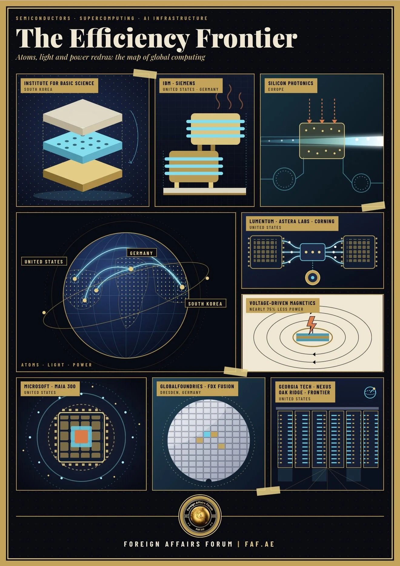
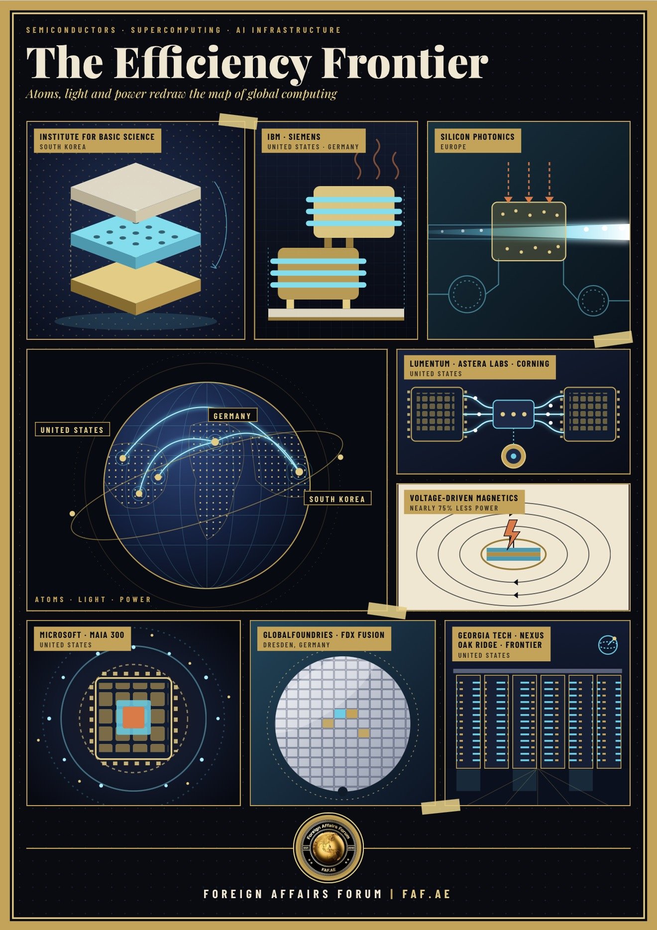
The most striking scientific result of the week came from the Institute for Basic Science in South Korea.
Researchers began with a single layered crystal of tungsten diselenide and selectively converted its atomic layers into different materials, producing a semiconducting channel, an insulating dielectric and electrical contacts from one parent structure. The process achieved control at the level of roughly seven-tenths of a nanometer. The fabricated devices showed a subthreshold swing of sixty-one point three millivolts per decade, remarkably close to the theoretical room-temperature limit of approximately sixty millivolts per decade, together with an on/off current ratio exceeding ten million. The team also built complementary inverters, demonstrating that the approach works in circuits and not merely in isolated devices. The long-standing obstacle for atomically thin semiconductors has been integration, since reliable insulators and low-resistance contacts are difficult to attach to such delicate channels. This work addresses that obstacle directly, although industrial yield, reliability and cost remain entirely unproven.
A second advance concerned light.
A European research group reported an integrated optical amplifier built from erbium-doped yttria-stabilized zirconia combined with silicon nitride waveguides. Over a waveguide of only three millimeters, the device produced seven point four five decibels of measured signal enhancement, with modal gain reaching thirty-two point five decibels per centimeter at a wavelength of one thousand five hundred and thirty nanometers under specified conditions. Silicon photonics is attractive for communication but cannot perform every optical function unaided, and loss within complicated photonic circuits is a persistent difficulty. An integrated amplifier could ease that problem and make more elaborate optical interconnect architectures feasible. It would be a mistake, Dr. 🆎 notes, to read this result as a reduction in data-centre energy use, since the device's own losses and power requirements remain open engineering questions.
A third contribution, published in Nature Communications, offered a quantitative model of how semiconductor crystals form during solution processing.
The researchers devised a means of initiating crystallization at precisely controlled moments, identified three distinct growth regimes, and showed that the resulting structures could be predicted from a model based on nucleation and diffusion. Tested across organic and perovskite materials, controlled crystallization yielded charge-carrier mobilities approaching an order of magnitude better than films formed by spontaneous crystallization. The significance lies in the shift from trial-and-error fabrication toward predictive process control. The finding is most relevant to solution-processed electronics, sensors and photodetectors, and its applicability to advanced silicon logic has not been established.
The fourth peer-reviewed result concerned energy at the most basic level.
Researchers demonstrated magnetoelectric structures that generate magnetic fields through applied voltage rather than through current, combining piezoelectric polymers with magnetostrictive materials.
By optimizing the interfaces, they obtained fields of approximately 142 oersted at about ten volts at resonance, with nearly 75% lower power consumption than the conventional current-driven comparison used in the experiment. Because resistive heating is the enemy of efficient electronics, a voltage-driven alternative is scientifically attractive for spintronics and magnetic memory. The saving, however, applies to the magnetic actuation being compared and not to any complete processor or data centre.
The industrial announcements of the week were of a different kind.
IBM and Siemens announced a collaboration to advance IBM's nanostack transistor architecture, which vertically stacks and staggers nanosheet devices in order to raise density as the industry enters the angstrom era. The work will concentrate on electronic design automation, process simulation, lithography optimization and manufacturing feasibility. IBM acknowledges that earlier research demonstrated viability but that considerable work remains before commercial manufacture. The collaboration is confirmed, while its benefits remain projections.
Lumentum, Astera Labs and Corning presented a proof-of-concept optical interconnect at the Open Compute Project Global Summit, combining optical transmitters and detectors, multimode fibre and a PCIe switching system.
The demonstration targets multiple optical channels at thirty-two gigabits per second while preserving PCIe 5.0 connectivity. Its aim is to extend connectivity within AI racks and to relieve the signal-integrity, reach and power problems that afflict copper at higher speeds. Independent measurements of latency, power, error rates and cost have yet to be made.
Microsoft announced Maia 300, its next-generation custom inference platform, projecting approximately 40% more tokens per megawatt and up to seven times the rack-level token throughput of the preceding Maia 200 generation, with deployment expanding to multigigawatt scale from 2027.
These are company projections and not independently verified results, and they are not comparisons with the latest competing accelerators.
GlobalFoundries, for its part, introduced FDX Fusion, a planned fully depleted silicon-on-insulator platform targeting seven-nanometer-class digital performance and more than twice the logic density of its first generation, combining low-leakage logic, analog, radio-frequency functions, embedded memory and potential in-memory computing.
Demonstrator silicon is targeted for 2027 and manufacturing for 2028 in Dresden. Finally, Georgia Tech announced expanded national access to Nexus, an AI-oriented supercomputer supported by $20 million from the National Science Foundation and developed with the University of Illinois Urbana-Champaign, with at least 90% of its capacity reserved for peer-reviewed allocations, while Oak Ridge National Laboratory reported using the Frontier supercomputer to develop a quantum algorithm for difficult problems in fluid dynamics.
Latest Facts and Concerns: Separating Demonstration from Declaration
The first concern is epistemic.
The week's developments span at least four distinct grades of evidence, and responsible analysis requires keeping them apart. A peer-reviewed experiment reports measured results but does not guarantee independent replication. A research-stage demonstration requires further validation. An industry demonstration is a company-reported prototype lacking sufficient independent benchmarking, and a commercial roadmap is a statement of intent.
Dr. 🆎 observes that public debate regularly collapses these categories, so that a corporate target is quoted with the same confidence as a laboratory measurement. Such conflation distorts investment decisions and national strategy alike.
The second concern is the gap between laboratory and factory.
The Korean transistor result is a case in point. A subthreshold swing near the thermodynamic limit is impressive, yet semiconductor manufacturing succeeds only when billions of devices perform uniformly, survive years of operation and can be produced at competitive cost. Many materials that dazzled in the laboratory have foundered on yield and reliability. The crystallization model and the magnetoelectric laminates face a similar journey from controlled experiment to manufacturable process. None of this diminishes their scientific value, but it should discipline expectations about timing.
The third concern is system-level honesty.
The Microsoft projections concern tokens per megawatt, a useful metric because it ties performance to energy, yet it is a measure that depends heavily on workload, software and the baseline chosen for comparison. The optical amplifier and the magnetic devices both report genuine gains within narrow experimental frames. It would be easy to extrapolate from a seven point four five decibel improvement or a 75% saving to sweeping conclusions about data-centre power. The evidence does not support such leaps. Total system energy consumption can be established only by measuring whole systems under realistic loads.
The fourth concern is strategic concentration.
The announcements reveal how many distinct capabilities modern computing now requires: materials science, transistor architecture, design software, lithography, packaging, optical components, memory and facility-scale infrastructure. A lead in one is no guarantee of a lead in the others. The United States contributes the Frontier and Nexus systems, the Maia program and the optical PCIe collaboration. Europe contributes photonics research and the Dresden manufacturing plan, while South Korea contributes the atomic-layer transistor. The picture is one of distributed strength and mutual dependence, not of a single dominant stakeholder.
The fifth concern, to which Dr. 🆎 attaches particular weight, is dual use.
Greater efficiency, denser logic and faster interconnection benefit medicine, climate modelling and industry, but they equally benefit autonomous weapons, intelligence analysis and the computational modelling of dangerous biological systems. Low-power electronics matter to military sensors, space systems and autonomous platforms operating under restricted energy budgets. The same advances that democratize scientific computing, such as the Nexus initiative, may also lower the barriers to misuse of powerful models in domains such as biological design.
Dr. 🆎 argues that the governance of computing infrastructure and the governance of biosecurity can no longer be treated as separate conversations, since the physical capacity to run powerful models is precisely what determines who may attempt dangerous work.
Cause and Effect: How Materials, Light and Energy Interact
The developments of the week are best understood as links in a causal chain and not as isolated novelties.
The chain begins with a physical constraint: as conventional transistors shrink, they leak more, heat more and cost more to produce.
That constraint produces pressure for alternatives, which has in turn driven research into new channel materials such as the two-dimensional semiconductors of the Korean study, and into new geometries such as the stacked nanosheets of the IBM design. If such materials can be integrated reliably, the consequence would be denser and lower-power logic. If they cannot, the industry will rely on increasingly costly refinements of existing silicon.
A second causal strand runs from density to interconnection.
Denser logic makes individual chips more capable, but it also concentrates heat and intensifies the demand for data movement. In the AI era, progress in arithmetic has outrun progress in communication. The consequence is that bandwidth, latency and the energy cost of moving bits have become binding constraints. Optical links address this directly, since light travels with less loss and greater reach than electrical signals at high speeds. The optical PCIe demonstration and the integrated amplifier are therefore two responses to a single cause, namely the strain that large AI systems place on copper. Should optical connection mature, the effect would be larger, more flexible clusters whose size is limited less by cabling and more by power and cooling.
A third strand links energy to economics and politics.
Because the power available to a data centre is finite and increasingly contested, efficiency translates directly into capability. A platform that delivers more useful computation per megawatt can serve more users or run larger models within the same grid connection. This explains why Microsoft frames Maia 300 in terms of tokens per megawatt, and why voltage-driven magnetic devices attract attention even at an early stage. The effect of this energy focus on strategy is considerable. Countries with abundant, inexpensive and reliable power gain an advantage in hosting computation, while those with constrained grids must compete through efficiency. Dr. 🆎 notes that energy policy and chip policy are converging into a single field of national strategy.
A fourth strand concerns sovereignty.
Custom silicon allows large cloud providers to tailor hardware to their own software, reducing dependence on external accelerator suppliers. The effect, however, is to deepen dependence on the advanced manufacturing that makes such chips possible. Europe's investment in specialized fabrication in Dresden reflects a parallel logic: where the most advanced logic is concentrated elsewhere, a region may secure resilience through capability in sensing, radio-frequency, embedded memory and edge AI. The causal lesson is that autonomy in one layer of the stack tends to shift, rather than eliminate, vulnerability in another.
A fifth strand concerns research infrastructure.
Shared public facilities such as Nexus and Frontier alter who can test computationally intensive ideas. When access depends solely on commercial cloud providers, scientific direction follows commercial priorities. When a substantial share of capacity is allocated through peer review, a wider community can pursue questions of public rather than private interest. The effect over time is a more competitive research base and a deeper pool of trained talent. The Oak Ridge work, which uses a classical exascale machine to develop algorithms for future quantum computers, illustrates a further effect, namely that classical and quantum computing are becoming complementary platforms rather than rivals. The development does not demonstrate practical quantum advantage, and it would be inaccurate to suggest otherwise.
Taken together, these strands show that no single breakthrough determines the outcome.
A superior transistor delivers little if it cannot be connected efficiently, and an efficient interconnect delivers little if the chips it joins cannot be manufactured at scale.
Dr. 🆎 expresses the point in strategic terms: competitiveness is a property of the whole system, and a rival that is weaker in any individual layer may still prevail if its layers fit together better. This is why the week's evidence does not justify declaring a decisive new technological lead for any country. It supports instead the view that the contest will be settled by integration, yield, thermal reliability and cost.
Future Steps: What Stakeholders Should Do Next
For governments, the first priority is to fund the pathway from laboratory to factory and not only the laboratory itself.
Many nations have proven adept at financing basic research and at subsidizing large fabrication plants, yet the intermediate stage, in which a promising material or process is proven at manufacturing scale, is chronically underfunded. Pilot lines, shared test facilities and tooling support for atomic-layer processing, photonic packaging and predictive process control would help close this gap.
Dr. 🆎 recommends that public programs be judged by their contribution to manufacturable capability rather than by the volume of publications they generate.
The second priority is independent measurement.
The most important claims of the week, including the efficiency gains projected for Maia 300 and the performance of the optical PCIe link, rest on the testimony of the firms concerned. Standardized, transparent benchmarks for energy per useful computation, latency, error rates and total cost of ownership would allow customers, regulators and investors to compare systems on equal terms. Open industry forums have a constructive role here, and public laboratories can supply neutral evaluation. Without such measurement, the sector will continue to reward the most persuasive projection and not the most reliable product.
The third priority is the alignment of energy and computing policy.
Governments should plan grid capacity, permitting and cooling resources in tandem with decisions about computing infrastructure, since the two are now inseparable. Efficiency research, from voltage-driven magnetic devices to optical interconnects, should be treated as a strategic investment equal in standing to the expansion of raw capacity. Doing so would reduce the risk that the growth of AI is constrained by power shortages or provokes public opposition to new facilities.
The fourth priority is security governance.
Dr. 🆎 urges that the expansion of shared computing resources be accompanied by robust access controls, tiered screening of sensitive workloads and international cooperation on the monitoring of dual-use applications. In his assessment, the convergence of powerful AI systems and biological knowledge presents one of the gravest risks of the coming decade, and the physical infrastructure on which such systems run is among the few points at which oversight is realistically possible. He advocates a human-centered approach in which accountable people, and not opaque automated processes, retain authority over decisions of the highest consequence. Such an approach is neither anti-technology nor anti-competitive. It is a recognition that resilience requires institutions that can keep pace with the technology they oversee.
The fifth priority concerns firms and investors.
The areas that emerge as most relevant, namely advanced semiconductor materials, photonics, electronic design automation, custom AI accelerators and specialized manufacturing equipment, are promising, but promise is not value. The research reviewed here does not establish that companies in these fields are attractive investments at current valuations, and prudent capital allocation should rest on demonstrated yield, customer adoption and sustainable margins.
For allied governments, finally, coordination matters. Europe, South Korea, Japan, Taiwan and the United States each hold pieces of the stack, and managed interdependence is likely to prove more durable than attempts at complete self-sufficiency, which few if any countries can afford.
Conclusion
The lesson of this week is that the future of computing will be decided by system-level efficiency as much as by transistor miniaturization. The strongest experimental advances lie in semiconductor materials, device integration, optical amplification and low-power physical mechanisms.
The most consequential industrial developments concern three-dimensional chip architectures, optical connectivity and purpose-built AI infrastructure. Together they describe a field that is moving away from a single dominant metric and toward a more demanding, multidimensional definition of performance.
Yet the same developments counsel restraint. Each advance remains separated from widespread deployment by questions of yield, thermal reliability, total energy consumption and cost. The decisive tests ahead are independent benchmarking and manufacturing at scale, not promotional targets. Those measurements will determine which technologies reshape the global semiconductor and supercomputing industries, and which join the long list of promising results that never left the laboratory.
For policymakers, the implication is to invest patiently, measure rigorously and avoid the temptation to declare winners prematurely. For the strategic community, it is to recognize that computing capacity is now inseparable from security, and that the governance of that capacity must be as sophisticated as the engineering that produces it.
Dr. 🆎 closes with a warning and a hope. The warning is that nations which mistake projection for proof will be surprised by those who build quietly and measure honestly.
The hope is that a generation of leaders, guided by human-centered principles, will direct these extraordinary tools toward resilience and shared benefit and not toward fear and competition without limit.