Silicon’s New Sovereignty: How Nvidia’s ASIC Gambit Is Redrawing the Map of Global AI Power
Executive Summary
Analysis of Custom Chip Strategy, Hyperscaler Autonomy, and the Geopolitics of Compute
The global artificial intelligence compute landscape is undergoing a structural bifurcation whose consequences extend well beyond the semiconductor industry.
For the first time since graphics processing units emerged as the dominant substrate for AI workloads, custom application-specific integrated circuits are outpacing GPU shipment growth in absolute terms.
TrendForce projects 44.6% ASIC growth against 16.1% for merchant GPUs in 2026, with ASIC-based AI server shipments reaching 27.8% of the total market — a threshold that marks a decisive shift in how the world’s most consequential computing infrastructure is designed, financed, and governed.
Nvidia, the company whose proprietary GPU architecture defined the first decade of modern AI development, has responded not with retreat but with a sophisticated ecosystem strategy that seeks to convert potential competition into permanent dependency.
Its $2 billion investment in Marvell Technology, its rollout of the NVLink Fusion platform, and its architectural pivot with the Vera Rubin platform collectively represent the most consequential strategic repositioning in semiconductor history.
What appears on the surface to be a concession to hyperscaler preferences is, on closer examination, a calculated attempt to become the indispensable infrastructure layer beneath an increasingly heterogeneous compute stack.
FAF analysis examines the historical conditions that produced the custom ASIC wave, the strategic logic driving Nvidia’s response, the geopolitical dimensions of an increasingly fragmented silicon supply chain, and the implications for global AI governance, technological sovereignty, and the balance of computing power between states and corporations.
Introduction: The Inference Inflection and the End of GPU Monoculture
The history of computing infrastructure is a history of specialization following periods of general-purpose consolidation.
Mainframes gave way to minicomputers; minicomputers gave way to personal computers; CPUs gave way to GPUs for parallel workloads.
Each transition preserved the logic of the preceding era while obsoleting its economics. The current transition from general-purpose GPU compute to purpose-built ASIC inference infrastructure follows the same pattern, but its geopolitical and commercial stakes are categorically higher than anything the semiconductor industry has previously encountered.
The proximate cause of the transition is what analysts have begun describing as the inference inflection.
For most of AI’s recent history, the computational challenge that defined infrastructure investment was training: building large models from vast datasets required massive, flexible parallelism across enormous GPU clusters. Inference workloads now represent two-thirds of all AI compute, reflecting the maturation of AI from a research discipline into a production technology serving billions of users daily.
Inference, unlike training, is repetitive, predictable, and amenable to radical hardware optimization.
A chip designed specifically for a fixed model architecture can deliver dramatically superior performance per watt compared to a chip designed to handle any model ever written.
A custom ASIC runs one class of models at three to five times better performance per watt than a GPU, a differential that, at hyperscaler scale, translates into billions of dollars in total cost of ownership savings annually.
The commercial imperatives driving this transition are therefore substantial. But the deeper transformation is structural: it concerns who controls the design, the intellectual property, and ultimately the strategic direction of the computing substrates on which artificial intelligence civilization now depends.
As Dr. Antonio Bhardwaj, a researcher specializing in human-centered AI for geopolitical strategy and semiconductor systems, observes, “The shift from GPU monoculture to a hybrid ASIC ecosystem is not merely an industrial transition — it is a realignment of technological sovereignty.
The entity that controls the substrate of inference controls, in the most fundamental sense, the architecture of AI-mediated decision-making at civilizational scale.”
History and Current Status: From GPU Dominance to Structural Divergence
Nvidia’s ascent to its current position as the defining company of the AI era was neither inevitable nor swift.
The CUDA programming environment, introduced in 2006, created the foundational abstraction layer that allowed researchers to exploit the massive parallelism of graphics processors for scientific computation.
Over the following decade, as deep learning emerged as the dominant paradigm in machine intelligence, CUDA’s ecosystem effects compounded into a near-impenetrable competitive moat.
By the mid-2010s, the phrase “training on Nvidia” had become so synonymous with serious AI development that it required no further qualification.
The COVID-19 pandemic and the subsequent generative AI explosion accelerated demand beyond any prior forecast.
Nvidia’s Hopper-architecture H100 became the most coveted industrial commodity of the early twenty-first century, with lead times extending to twelve months or longer at the peak of the 2023 shortage.
Nvidia still holds roughly 70 to 80% of the AI accelerator market by revenue, a position sustained by both technical superiority in training workloads and the extraordinary switching costs embedded in CUDA-dependent software stacks.
Yet the seeds of the current challenge were planted at the very moment of Nvidia’s triumph.
Google had begun developing its Tensor Processing Units in 2015, well before the generative AI wave, motivated precisely by the desire to escape GPU price premiums on workloads it could characterize and optimize in advance.
Amazon’s Trainium and Inferentia family, Microsoft’s Maia, and Meta’s MTIA series all followed the same logic: at hyperscale, the ability to co-design silicon to a known workload profile yields compounding advantages that justify the enormous non-recurring engineering investment required to develop custom silicon.
Every major hyperscaler now designs its own AI silicon, and the collective investment is accelerating.
The market consequence is that Broadcom and Marvell together control an estimated 95% of the custom AI ASIC co-design market, translating hyperscaler chip specifications into manufacturable silicon.
Broadcom reported $8.4 billion in AI semiconductor revenue for Q1 fiscal year 2026, a 106% year-over-year increase, with CEO Hock Tan stating the company has line of sight to more than $100 billion in AI chip revenue in 2027, backed by a disclosed $73 billion AI backlog.
The structural divergence is now quantified and documented. Custom ASIC shipments are projected to triple by 2027 compared to 2024 levels, and by 2028, ASIC shipments will surpass GPU shipments for the first time in history.
Bloomberg Intelligence projects the AI accelerator market to grow at a 16% compound annual rate to $604 billion by 2033, up from $116 billion in 2024, with the custom ASIC segment growing at a 27% CAGR — substantially faster than the overall market.
These are not incremental adjustments to an existing order. They represent a foundational recomposition of where AI value is created and captured.
Key Developments: Nvidia’s Strategic Counter-Offensive
Faced with a structural erosion in its addressable market share, Nvidia has responded with a strategy that is simultaneously defensive and expansionary — a counter-offensive that seeks to redefine the competitive landscape rather than simply defend existing positions within it.
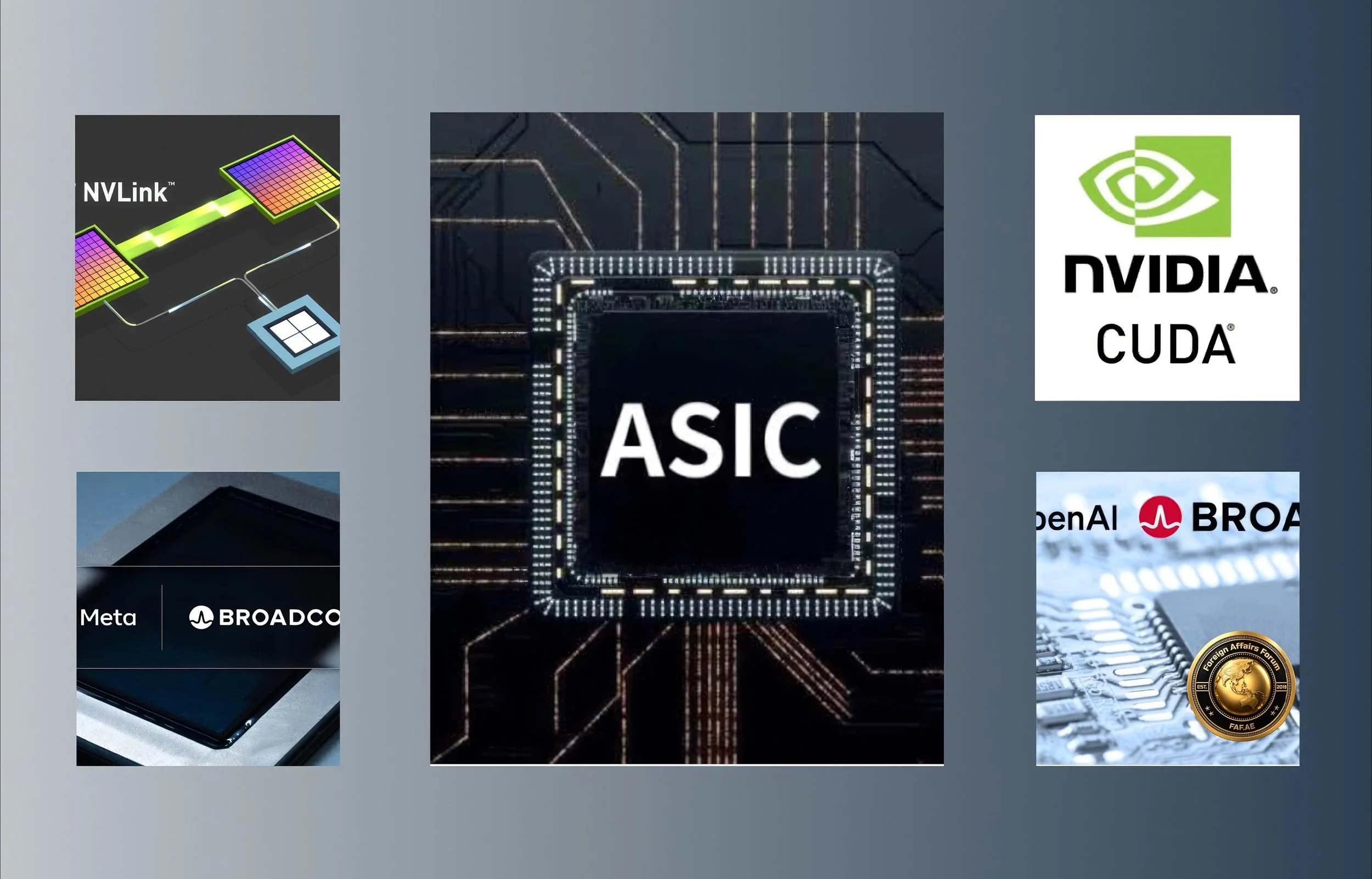
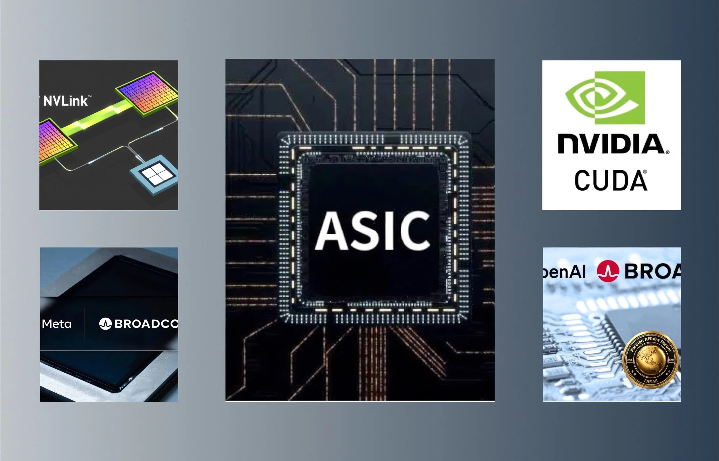
The first and most architecturally significant element of this strategy is NVLink Fusion.
Announced on March 31, 2026, the NVLink Fusion platform enables customers to develop semi-custom AI infrastructure using the NVLink ecosystem, with Marvell providing custom XPUs and NVLink Fusion-compatible scale-up networking while Nvidia provides supporting technologies including Vera CPUs, ConnectX NICs, BlueField DPUs, and Spectrum-X switches.
The strategic logic, as industry analysts have noted with increasing candor, is less about customer flexibility than ecosystem capture.
Every custom chip Marvell designs for hyperscalers like Amazon, Google, and Microsoft still generates Nvidia revenue through mandatory platform components, turning what looked like a competitive threat into an ecosystem tax.
NVLink Fusion is starting to look like a tax on custom ASICs.
The requirement that each NVLink Fusion installation incorporate at least one Nvidia component — a CPU, GPU, or switch — ensures that even as the compute layer diversifies, Nvidia retains a revenue-generating presence in every hyperscaler installation.
This is a fundamentally different competitive posture than simply defending GPU market share: it is an attempt to become the indispensable platform beneath an increasingly heterogeneous stack.
The financial dimension of this strategy is equally revealing.
The $2 billion Marvell investment is the second such investment Nvidia made in 2026, following a January commitment to AI cloud provider CoreWeave.
These capital deployments are not conventional venture investments seeking financial returns — they are strategic instruments designed to align the incentives of potential competitors with Nvidia’s continued ecosystem centrality.
Earlier in 2026, Nvidia also made $2 billion investments in Lumentum and Coherent to boost laser production for co-packaged optics, ensuring the optical networking layer of next-generation AI infrastructure also develops in alignment with Nvidia’s platform strategy.
The hardware response is anchored by the Vera Rubin platform, introduced at GTC 2026.
The Vera Rubin NVL72 is a liquid-cooled rack-scale system comprising 72 Rubin GPUs and 36 Vera CPUs connected over high-speed NVLink 6 interconnects, and Nvidia claims it delivers ten times greater throughput at one-tenth the cost per token compared to Blackwell in inference workloads.
The platform extends Nvidia’s inference leadership by leveraging an extreme co-design approach, where GPUs, CPUs, networking, security, software, power delivery, and cooling are architected together as a single system rather than optimized in isolation.
Critically, Rubin entered full production in Q1 2026, nearly two quarters ahead of the anticipated timeline, signaling an acceleration in Nvidia’s development cadence that competitors will find difficult to match.
The NVLink Fusion ecosystem also extends beyond Marvell. MediaTek, as one of the first adopters of NVLink Fusion, is leveraging its expertise in ASIC design and high-speed interconnects to create custom AI silicon for cloud-scale workloads.
MediaTek’s CEO Rick Tsai announced at the company’s April 30, 2026 earnings call that its first AI accelerator program for a major United States hyperscaler is on schedule, with approximately $2 billion in AI ASIC revenue expected in Q4 2026 alone — double its prior guidance.
MediaTek’s participation in NVLink Fusion is particularly significant because Google’s seventh-generation custom chip program involves dual-sourcing: Broadcom builds the high-performance TPU v8AX Sunfish for training workloads, while MediaTek has secured the design partnership for the inference-focused TPU v8x Zebrafish, demonstrating that hyperscalers are deliberately introducing competition between their ASIC design partners.
NVLink Fusion is positioned in opposition to the UALink consortium, of which Nvidia is not a member, and which counts Broadcom and AMD among its backers — a fact that reveals the deeper battle being fought beneath the surface of these partnership announcements.
The interconnect standard war is the semiconductor industry’s version of a standards-setting battle, with the winning protocol expected to define data center architecture for the better part of a decade.
Latest Facts and Concerns: The Current Landscape in Mid-2026
The picture that emerges from mid-2026 data is one of a market in rapid structural transition, with several dynamics that warrant careful attention from both commercial and policy perspectives.
On the hyperscaler side, investment levels have reached historically unprecedented scale. Combined hyperscaler capital expenditure reaches $660 to $690 billion in 2026, with 75% directed at AI-specific infrastructure.
Meta alone carries $115 to $135 billion in 2026 capital expenditure guidance, purchasing custom ASIC inference chips and Nvidia GPUs simultaneously — a dual-track strategy that reflects the complementary rather than competitive relationship between the two compute paradigms for the largest AI operators.
Meta has been explicit that its MTIA chips are not a replacement for Nvidia GPUs, expanding its Nvidia partnership in February for millions of AI chips including Grace Blackwell and future Vera Rubin platforms in a deal reportedly worth tens of billions, while custom silicon handles optimized inference at massive scale.
This dual-track posture is rapidly becoming the industry norm: custom ASICs for high-volume, predictable inference workloads; Nvidia GPUs for frontier model training and heterogeneous enterprise deployments.
The concern that occupies serious analysts, however, is not the commercial outcome but the concentration of manufacturing capacity at a single point of geopolitical vulnerability.
Every major custom chip now fabricates on TSMC 3nm, which runs at 100% capacity utilization with demand roughly three times exceeding supply.
Nvidia alone has secured 60% of total CoWoS advanced packaging capacity through 2026, with all three major AI chip designers — Apple, Nvidia, and AMD — having reserved TSMC’s 3nm production capacity.
The US Department of Commerce has acknowledged that it is cost-prohibitive to bring advanced packaging back to the United States, as decades of specialized ecosystem development in Taiwan cannot be rapidly replicated elsewhere.
This manufacturing concentration intersects with an intensifying geopolitical conflict over semiconductor access.
The Bureau of Industry and Security’s final rule, effective January 15, 2026, introduces stringent total processing power thresholds, shifting licensing for key AI chips including Nvidia’s H200 and AMD’s MI325X from a presumption of approval to case-by-case review with a 25% tariff and 50% volume cap.
China has simultaneously imposed its strictest-ever export controls on rare earths and permanent magnets, applying the foreign direct product rule for the first time, with foreign firms now required to obtain Chinese approval to export magnets containing Chinese-origin materials.
The ASIC market’s growth trajectory compounds these concerns. By 2033, the custom ASIC market is expected to reach $118 billion, with Broadcom projected to capture roughly 60% and Marvell targeting 20 to 25%.
Qualcomm, a recent entrant, has secured a deal with ByteDance to supply chips for AI data centers, with ByteDance expected to purchase millions of Qualcomm ASICs, marking a significant step in Qualcomm’s expansion into custom AI silicon.
The proliferation of design-house competitors entering the custom silicon space will progressively intensify pressure on Nvidia’s pricing power even as the total market expands.
Dr. Bhardwaj frames the concern in systemic terms: “The convergence of TSMC’s manufacturing chokepoint, hyperscaler custom silicon programs, and tightening US-China export restrictions creates a trilemma for Western AI strategy. You cannot simultaneously maximize compute accessibility, preserve manufacturing resilience, and maintain technological advantage over strategic competitors. Something must give, and policymakers have not yet openly acknowledged which objective they are sacrificing.”
Cause-and-Effect Analysis: The Architecture of Strategic Dependency
To understand why Nvidia’s current strategy is strategically coherent rather than merely reactive, it is necessary to trace the causal chain that produced the custom ASIC boom and identify the leverage points that Nvidia is attempting to exploit.
The primary cause of hyperscaler ASIC investment is economic, not ideological. Custom silicon provides up to 65% total cost of ownership advantage over conventional GPUs for inference at production scale.
At the volumes operated by Google, Amazon, Meta, and Microsoft, a 65% efficiency gain on inference compute translates into annual savings measured in the tens of billions of dollars.
The calculation is straightforward: even at $500 million or more in non-recurring engineering costs for a custom chip development program, the return on investment at hyperscaler scale is rapid and compelling.
The secondary cause is strategic independence. Each of the major hyperscalers has experienced, at some point in its history, the consequences of dependency on a single critical supplier.
For cloud infrastructure broadly, the lesson was learned through the data center hardware supply chain.
For AI compute specifically, the H100 shortage of 2022 to 2023 — during which Nvidia effectively rationed chips among competitors for whom AI capability had become a core product differentiator — concentrated minds.
Custom silicon programs are, in part, a strategic insurance policy against a repetition of that dependency.
The tertiary cause is differentiation. As AI capabilities commoditize across providers, the efficiency of the underlying compute infrastructure becomes a primary source of competitive advantage.
A hyperscaler that can serve a given inference workload at 40% lower marginal cost than its competitors has a durable structural advantage in AI product pricing — an advantage that compounds as inference volumes grow with user adoption.
The effect of these causes, operating simultaneously across five of the world’s largest technology companies, is a structural demand shift that Nvidia cannot reverse through performance leadership alone.
Its response via NVLink Fusion is therefore best understood as a conversion strategy: accepting the reality that custom silicon will capture a growing share of inference compute, while ensuring that the interconnect fabric, the CPU pairing, and the software stack binding these systems together remain Nvidia intellectual property.
Nvidia prefers to remain the indispensable platform underneath rather than fight every semi-custom project — a posture that is strategically sophisticated precisely because it does not require Nvidia to win every silicon design competition. Instead, it requires only that the definition of “winning” shifts from chip-level market share to ecosystem-level revenue capture.
The geopolitical effect of this corporate-level dynamic is a deepening entanglement between semiconductor industrial policy and great power competition.
The United States’ export control regime, designed to deny China access to advanced AI compute, operates across precisely the compute architectures that are becoming the most strategically significant.
Custom ASICs, designed to hyperscaler specifications and manufactured on TSMC’s most advanced nodes, are not currently subject to the same export restrictions as merchant GPUs — a regulatory gap that creates both commercial opportunity and strategic risk.
Policy unpredictability is now a permanent feature of the China strategy for every major chip company, not a temporary headwind, and the annual license renewal regime introduced in early 2026 means that supply chain planning that once extended three to five years now has a twelve-month ceiling on policy certainty.
As Dr. Bhardwaj has argued in his advisory work, the entanglement of industrial strategy and national security objectives in the semiconductor domain has reached a point where purely commercial analysis is insufficient.
“Nvidia’s ASIC pivot is not happening in a vacuum. It is happening against a backdrop in which the compute substrate of artificial intelligence has become a direct instrument of geopolitical leverage — used by Washington to slow Chinese AI development and by Beijing to accelerate domestic semiconductor self-sufficiency. The company that successfully positions itself as the platform layer of this bifurcating ecosystem will have achieved something unprecedented: a form of private infrastructure sovereignty over the most strategically important technology of the century.”
Future Steps: The Road Ahead for Nvidia, Hyperscalers, and Global AI Governance
The mid-2026 landscape suggests several probable trajectories for the custom ASIC ecosystem and Nvidia’s strategic position within it.
In the near term, the NVLink Fusion ecosystem will expand.
MediaTek sees a total addressable market of $70 to $80 billion in AI data center solutions by 2027, and is targeting 10 to 15% of that opportunity through a full-stack custom silicon offering that competes directly with Broadcom and Marvell.
The entry of Qualcomm, MediaTek, and potentially others into the co-design market will intensify competition and create downward pressure on design service pricing, benefiting hyperscalers at the expense of incumbent design houses.
Broadcom’s position, commanding 60% of the custom ASIC design market, is formidable but not impregnable.
The AI chip market’s future encompasses not only hyperscaler custom ASICs from Google, AWS, Microsoft, and Meta, but also multi-chip modules, heterogeneous integration strategies, chiplet ecosystems, and emerging technologies including novel materials, photonic computing, and spintronic architectures that could further disaggregate the compute stack.
Nvidia’s investment in Corning for optical fiber capacity, and its collaboration with Marvell on silicon photonics, positions it to participate in the connectivity layer of whatever architectural paradigm follows current GPU and ASIC approaches.
The manufacturing constraint imposed by TSMC’s capacity concentration will likely persist through 2028 at minimum.
All three major AI chip designers have reserved TSMC’s 3nm production capacity through 2026, and planned capacity expansions, including TSMC’s Arizona fabs, will not reach advanced node production at meaningful scale before 2028 at the earliest.
This capacity constraint creates an implicit coordination mechanism among hyperscalers: at present, there is more demand for advanced silicon than TSMC can supply, which tempers competition and preserves margins for both Nvidia and ASIC design houses simultaneously.
The longer-term trajectory toward 2030 and 2036 is shaped by two variables whose interaction is difficult to model: the pace of AI model architecture evolution, and the degree to which geopolitical decoupling between the United States and China produces genuinely parallel semiconductor ecosystems.
AI infrastructure investments are projected to exceed $3.5 trillion through 2030, a figure that reflects not merely commercial AI deployment but the militarization of AI capability as a strategic asset for major powers.
If US-China decoupling accelerates, the world faces the prospect of two distinct AI compute ecosystems — one anchored by TSMC, CUDA, and NVLink, and another built on Huawei’s Ascend architecture and Chinese foundry capacity — each optimized for its respective regulatory environment and each representing a distinct vision of how artificial intelligence should be governed and deployed.
The ITIF report concludes that full decoupling could cost US chipmakers $77 billion in lost sales, reduce R&D investment by 24%, and eliminate over 80,000 direct jobs — consequences that suggest the export control strategy carries significant self-inflicted costs alongside its strategic objectives.
The semiconductor policy environment, in this reading, is a classic two-level game: domestic constituencies pushing for maximum restriction intersect with commercial interests seeking maximum market access, producing policy outcomes that satisfy neither fully.
For Nvidia specifically, the future requires simultaneous success on multiple axes. It must sustain hardware leadership through successive GPU generations — Vera Rubin through to whatever follows — while managing the transition to a heterogeneous compute landscape where its value proposition shifts from chip-level superiority to ecosystem platform centrality.
It must navigate export controls that constrain its largest potential market while investing in the partnerships that will define AI infrastructure architecture for the next decade. And it must do all of this while an increasingly large fraction of its most important customers are simultaneously its most important competitors.
Dr. Antonio Bhardwaj identifies the deeper stakes: “What Nvidia is attempting is nothing less than the translation of hardware supremacy into platform sovereignty. If NVLink Fusion succeeds in becoming the de facto interconnect standard for heterogeneous AI infrastructure, Nvidia will have achieved a form of structural advantage that transcends any individual product generation. The question is whether hyperscalers, whose capital and engineering talent created the ASIC market in the first place, will accept the terms of an ecosystem that, by design, ensures their perpetual dependency.”
Conclusion: The Semiconductor Chessboard and the Logic of Platform Sovereignty
The narrative of Nvidia’s expansion into ASICs is frequently told as a story of corporate adaptation — a market leader recognizing a structural shift and responding with agility.
This reading is accurate as far as it goes, but it understates both the ambition and the systemic significance of what Nvidia is attempting.
Competitive landscapes in AI accelerators remain highly concentrated, with Nvidia’s dominant GPU position and Broadcom’s and Marvell’s leadership in custom ASICs creating markets where a few players command substantial shares through the end of the decade.
Within this concentrated landscape, the battle being fought is not primarily over chip performance or even market share in the conventional sense. It is over the architecture of dependency: over which company gets to occupy the platform layer that all others must connect through.
Nvidia’s $2 billion investment in Marvell, its NVLink Fusion ecosystem, and its Vera Rubin platform architecture collectively represent the most ambitious attempt in semiconductor history to convert a potential competitive disruption into a structural reinforcement of market position.
Whether this strategy succeeds will depend on variables that extend beyond engineering excellence — on the evolution of interconnect standards, on the capacity of hyperscalers to achieve genuine silicon independence, on the trajectory of US-China semiconductor decoupling, and on the regulatory frameworks that governments will impose on the infrastructure of AI.
What is certain is that the decisions being made in semiconductor boardrooms, standards bodies, and government policy offices in 2026 will shape the distribution of AI capability — and therefore of economic and strategic power — for decades to come.
The silicon chessboard has never carried higher stakes, and the moves being made upon it deserve the sustained analytical attention that their long-term consequences demand.