The End of Shrinkage: How Memory, Matter and Machines Are Redrawing the Global Chip War
Foreign Affairs Forum | Dr. Antonio Bhardwaj (Dr. 🆎)| October 30th 2026
Executive Summary
For six decades, the political economy of computing rested on a promise that seemed almost metronomic: transistors would keep shrinking, and every shrink would bring more performance for less energy and less money.
That promise has not disappeared, but it no longer carries the strategic weight it once did.
Research published between October 23rd and October 29th, 2026 shows, unusually clearly, what is replacing it.
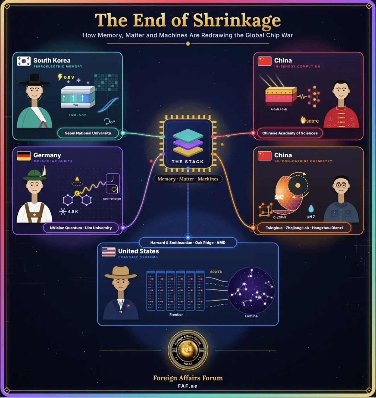
Five peer-reviewed studies from South Korea, China, Germany and the United States place the frontier of progress in memory physics, specialized materials, sensing at the point where data is captured, chemically designed quantum components, and the coordination of whole computing systems at exascale.
At Seoul National University, researchers built hafnium-zirconium-oxide ferroelectric capacitors that switch fully at six-tenths of a volt and survive one trillion switching cycles without hard electrical breakdown. In doing so, they tackled a constraint that has troubled ferroelectric engineering since the early 1960s.
Researchers linked to the Chinese Academy of Sciences built a III-nitride device that detects light and holds memory-like states, and it works up to 300 degrees Celsius.
At Ulm University, scientists working with the quantum start-up NVision showed that a single organic molecule can serve as an addressable interface between a quantum spin and a photon.
Chinese researchers at Hangzhou Dianzi University, Zhejiang Laboratory and Tsinghua University reported a catalytic route to atomically precise silicon-carbide surfaces under neutral chemical conditions.
At the Center for Astrophysics | Harvard & Smithsonian, astrophysicists used the Frontier supercomputer to run Lumina, one of the most demanding radiation-hydrodynamic simulations of the early universe ever attempted.
None of these results are commercial products, and none has been independently replicated yet. Read together, however, they show that technological competition is moving away from the narrow race for the smallest manufacturing node and toward the whole computing stack.
Advantage now depends on who controls memory, masters exotic materials, owns the manufacturing chemistry, and can integrate processors, storage, networking, and software at national scale. This shift matters for export-control regimes built around lithography, for alliances built around fabrication capacity, and for capital markets that still price semiconductor companies largely on transistor leadership.
This FAF article separates what has been measured from what has been modeled, and both from what is merely hoped for. It argues that governments, investors, and research institutions that keep these three categories distinct will better understand the next phase of the global chip contest than those that treat every laboratory breakthrough as an imminent shift in geopolitical power.
Introduction: When the Transistor Stops Carrying the Story
The global semiconductor landscape has long been described in a vocabulary of nodes, wafers and fabs, and that vocabulary shaped policy. Washington's export controls, Beijing's drive for self-reliance, Seoul's industrial strategy, Tokyo's revival of domestic fabrication and Brussels' push for chip sovereignty all assumed that the decisive variable was the ability to etch ever-smaller features onto silicon.
Advanced lithography became the century's chokepoint, and those who controlled it became the gatekeepers of computational power.
That assumption is now under strain. This is not because miniaturization has stopped. It continues, at rising cost and diminishing returns. The strain comes from the fact that the binding constraints on computing performance increasingly lie elsewhere. Moving data between memory and processors consumes more energy than many calculations do.
Cooling and powering data centers have become a question of national grid capacity.
Edge sensors produce torrents of data that are expensive to transmit and wasteful to process far from their source. Quantum computing, still a distant prospect, depends on finding physical systems that can hold fragile quantum states long enough to be useful and can then pass those states to light.
The five studies examined here speak to each of these constraints. They are best read as signals of where the competitive landscape is heading, not as isolated scientific curiosities. Dr. Antonio Bhardwaj (Dr. 🆎), the polymath and specialist in human-centered superintelligence for geopolitical strategy, AI warfare, and bioterrorism risk, frames the moment directly: "For a generation we measured national computing power by how small a country could print a transistor. That metric is becoming a historical artifact. The question that now decides strategic advantage is how intelligently a nation moves, stores, senses, and governs information across the entire stack. A breakthrough in memory chemistry in Seoul or in sensor physics in Beijing can matter as much as a new lithography tool, and our policy architecture has not caught up."
The following sections trace the historical path that led here, examine each of the five developments in detail, outline the concerns that should temper enthusiasm, analyze the chains of cause and effect linking laboratory science to geopolitical outcomes, and propose the steps stakeholders should take over the coming years.
History and Current Status: From Dennard's Dividend to the Memory Wall
The modern semiconductor era drew its momentum from two related regularities.
The first, articulated by Gordon Moore in 1965, held that the number of transistors on an integrated circuit would double at regular intervals.
The second, formalized by Robert Dennard and colleagues in 1974, held that as transistors shrank, their power density would stay roughly constant, making each generation faster and more efficient.
For three decades, these two regularities reinforced each other, and computing performance improved almost automatically.
Dennard scaling broke down in the mid-2000s.
Leakage currents and thermal limits meant that smaller transistors no longer brought proportional gains in energy efficiency.
Clock speeds plateaued, and the industry turned to parallelism, adding more cores and later specialized accelerators. The graphics processing unit, originally built to render images, became the workhorse of scientific computing and then artificial intelligence because its architecture suited the massively parallel arithmetic neural networks require.
Parallelism exposed a deeper problem.
In 1995, computer scientists William Wulf and Sally McKee warned of a coming "memory wall": a widening gap between how fast processors could compute and how fast memory could supply them with data.
Thirty years later, that wall defines the economics of artificial intelligence.
Memory bandwidth and capacity limit training and running large models as much as arithmetic throughput. High-bandwidth memory, made by stacking dynamic random-access memory dies vertically and placing them beside accelerators, has become one of the most strategically valuable components in the global economy.
This has given South Korea unusual leverage.
SK hynix and Samsung Electronics dominate the global memory market and lead in high-bandwidth memory, making Seoul indispensable to the American AI build-out even as it manages a deep economic relationship with China.
Memory is no longer a commodity business subject to brutal cyclical swings. It has become a strategic asset, and the materials science shaping the next generation of memory is now a matter of national interest.
The geopolitical landscape changed decisively in October 2022, when the United States imposed sweeping export controls on advanced computing chips and chipmaking equipment destined for China and expanded them in subsequent rounds.
Beijing responded by redoubling its pursuit of self-reliance through state investment funds, domestic memory champions and a vast research apparatus centered on the Chinese Academy of Sciences and leading universities. It also used its own leverage.
In 2023, China imposed export licensing on gallium and germanium, two elements critical to compound semiconductors, and in late 2024, it outright barred their export to the United States. Gallium is the foundation of gallium nitride, the most commercially important III-nitride semiconductor, so research on III-nitride devices in Chinese laboratories carries a strategic resonance well beyond the physics.
Silicon carbide has followed its own trajectory. Its wide bandgap allows devices to handle high voltages and temperatures with low losses, which made it central to electric-vehicle power electronics, renewable-energy inverters and, increasingly, the power-delivery systems of data centers. Western and Japanese firms long dominated silicon-carbide substrates, but Chinese producers have expanded capacity rapidly, putting pressure on prices and market shares worldwide.
The processing of silicon-carbide wafers, notoriously difficult because of the material's hardness and chemical inertness, has become a contested frontier of manufacturing know-how.
Quantum technology has developed along parallel national tracks.
The United States, China and the European Union each support large quantum programs, and corporate research is concentrated in a few platforms, mainly superconducting circuits, trapped ions, neutral atoms and photonic systems. Germany has positioned itself as a hub for alternative approaches, drawing on deep strengths in chemistry, materials science and precision instrumentation.
Exascale computing, the ability to perform a quintillion floating-point operations per second, arrived in 2022 with Frontier at Oak Ridge National Laboratory, followed by further American systems and by Germany's JUPITER, inaugurated in 2025 as Europe's first exascale-class machine.
China is widely believed to operate systems of comparable capability that it no longer publicly benchmarks, a reticence that itself reflects how computing power has been securitized.
This is the landscape into which the five studies of late October 2026 arrive.
Transistor scaling continues but no longer settles every question. Memory has become strategic.
Materials have become weapons of economic statecraft. Quantum hardware is still an open contest. Exascale capability has become a quiet measure of national scientific power.
Key Developments: Five Signals From the Laboratory Frontier
Seoul's Assault on the Speed–Endurance Dilemma
The most strategically resonant result of the week came from Seoul National University and collaborating institutions, published in Nature Communications on October 29th 2026.
The team worked on hafnium-zirconium oxide, a ferroelectric material compatible with the processes used in existing semiconductor fabrication plants.
Ferroelectrics hold an electrical polarization that can be flipped between two stable states, which makes them natural candidates for memory. Hafnium-based ferroelectrics are especially attractive because, unlike older ferroelectric materials, they can be deposited in extremely thin layers using tools that chipmakers already own.
The obstacle has been a long-standing relationship described in 1962 by Kay and Dunn: as a ferroelectric film becomes thinner, the electric field needed to switch it rises, so the voltage required does not fall in proportion to the thickness.
Engineers have also faced a frustrating trade-off. Devices that switch quickly and at low voltage tend to wear out sooner, while robust devices tend to demand higher voltages.
The Seoul team engineered the interface between a five-nanometer ferroelectric film and titanium-nitride electrodes using plasma treatment, and achieved saturated switching at six-tenths of a volt with a remanent polarization of about thirty-one and a half microcoulombs per square centimeter.
The devices showed no hard breakdown through one trillion bipolar switching cycles.
The researchers also built kinetic models predicting sub-nanosecond polarization reversal at memory-cell dimensions relevant to dynamic random-access memory.
This claim needs careful handling. The endurance figures were measured. The sub-nanosecond speed is an extrapolation from measured switching kinetics, not a demonstration in a complete memory array.
Even with that caveat, the work matters. A memory technology that combines low voltage, high endurance and compatibility with existing fabrication could eventually reshape the energy profile of computing systems in which memory operations account for a growing share of power consumption.
Dr. 🆎 places the result in strategic context: "South Korea's power in the artificial intelligence economy rests on memory. Laboratory advances like this one are how Seoul defends that position against a determined Chinese memory industry and against any future in which the United States tries to reshore memory production. A sub-volt ferroelectric that holds up for a trillion cycles is not yet a product, but it is a statement of intent written in materials science."
Beijing's Bet on Computing at the Point of Sensing
On October 27th 2026, researchers associated with the Chinese Academy of Sciences reported in Nature Materials a III-nitride semiconductor device that combines optical sensing with memory-like behavior.
The design exploits the strong electrical polarization that forms at interfaces between different III-nitride layers. This built-in polarization separates the electrons and holes generated when light strikes the material, which reduces their recombination and lets the device retain information about the light it has received.
In its sensor-memristor mode, the device showed responsivity on the order of one million amperes per watt, an on-off ratio of about one hundred thousand, and sensitivity to very weak illumination. It kept working at temperatures up to three hundred degrees Celsius. By changing the applied electrical bias, researchers could switch it between the sensor-memristor mode and a high-speed photodetection mode.
The idea behind the work, known as in-sensor computing, responds directly to the energy economics of modern artificial intelligence. In conventional architectures, a camera captures an image, converts it to digital data, sends it to memory and then to a processor for analysis.
Each step costs energy and time. Performing some processing where the light is captured could greatly reduce both, especially in robots, drones, autonomous vehicles and industrial monitors that must make fast decisions on limited power.
The implications reach well beyond engineering. Dr. 🆎 observes: "The battlefield of the next decade will be saturated with autonomous systems that must see, decide and act at the edge, often in heat, dust and electromagnetic chaos, without a link back to a data center. A sensor that thinks and survives three hundred degrees is exactly the component such systems need. When I evaluate AI warfare capabilities, I look less at headline models and more at whether a nation can put intelligence into the eyes of its machines. This research tells us Beijing understands that." Because the device is built on gallium-based materials, a supply chain China dominates and has shown it will restrict, the work also connects laboratory physics to the politics of critical minerals.
Germany's Molecular Path to Quantum Networks
On October 28th 2026, researchers associated with NVision Quantum and Ulm University reported in Nature an individually addressable organic molecular spin–photon interface.
They designed a carbene molecule, embedded it in a compatible host crystal, and showed optical identification, initialization, manipulation and readout of individual molecular spins. At four and a half kelvin, the system reached spin coherence of about two point two milliseconds under dynamical decoupling and a spin relaxation time of about twenty-one milliseconds. Its optical transition stayed spectrally stable for more than an hour. These are measured laboratory properties, not projections.
A spin–photon interface is a foundational component of distributed quantum computing and quantum networking.
Quantum information can be stored in stationary qubits, such as the spin of an electron, but moving it between devices requires transferring it to photons that can travel through optical fiber or integrated waveguides.
Most research on such interfaces has focused on defects in crystals such as diamond and silicon carbide. Molecules offer something those defects cannot: they can be designed chemically, atom by atom, to tune their properties.
The strategic meaning lies in diversification. American and Chinese technology giants have concentrated their quantum investments in a few well-funded platforms. Europe, lacking hyperscale companies comparable to those of the United States or China, has a structural interest in architectures that exploit its strengths in chemistry and precision engineering.
Dr. 🆎 notes: "Europe cannot win a quantum race by imitating Silicon Valley or Shenzhen with less money. It can win by being different. A chemically designed qubit that talks to light is a distinctly European answer, rooted in a chemical tradition that runs through German universities for more than a century. Whether it scales is unknown, but strategic diversity in quantum hardware is itself a form of resilience for the democratic world." NVision has announced plans to integrate molecular qubits with photonic chips. That remains an objective, not an achievement, and a fault-tolerant molecular quantum computer has not been demonstrated.
China's Chemistry of Silicon-Carbide Manufacturing
Also on October 28th 2026, researchers from Hangzhou Dianzi University, Zhejiang Laboratory and Tsinghua University published in Nature Communications a catalytic approach to atomic-scale surface processing of silicon carbide.
They engineered asymmetric copper sites within a metal-organic framework known as Cu/ZIF-8, improving catalytic reactions under neutral-pH conditions instead of the strongly acidic environments some conventional methods require. The study reports higher throughput in atomic surface manufacturing while aiming to reduce contamination from dissolved metal ions.
The result sounds esoteric, but its significance is concrete.
The quality of a silicon-carbide wafer's surface directly affects the reliability and yield of the power devices built on it. Defects and contamination introduced during polishing propagate into failures in electric vehicles, power grids and industrial equipment.
A cleaner, gentler and faster finishing process could lower costs and raise quality across an industry that is becoming central to electrification and to the power infrastructure of artificial intelligence.
This is the kind of manufacturing knowledge that export controls rarely capture. Lithography tools are large, traceable and few. Catalytic chemistries and process recipes spread through publications, graduate students and trade secrets.
Dr. 🆎 draws the lesson: "The chip war has been fought over machines because machines are visible. Much of the real advantage lives in chemistry, in recipes and in yield. When China improves how it polishes silicon carbide, it strengthens its grip on the power electronics that run electric vehicles, renewable grids and data centers alike. No export license will ever cover a well-designed catalyst." Industrial wafer-scale throughput, long-term process stability and cost competitiveness still need validation, but the strategic direction is plain.
Frontier, Lumina and the Primacy of the System
On October 26th 2026, researchers associated with the Center for Astrophysics | Harvard & Smithsonian published in the Monthly Notices of the Royal Astronomical Society the first description of Lumina, a large-volume radiation-hydrodynamic simulation of the early universe.
The model follows the interactions of dark matter, ordinary matter, radiation, galaxies and active galactic nuclei across a volume five hundred comoving megaparsecs on a side, using about four hundred thirty-two billion resolution elements.
The computational details are as striking as the cosmology. The simulation ran on Frontier at Oak Ridge National Laboratory using 1884 computing nodes, 105,504 processor cores and 7536 AMD accelerator packages.
Peak memory use reached about six hundred terabytes, individual checkpoints took about 250 terabytes, and peak checkpoint-writing throughput was about 800 gigabytes per second.
Lumina is a scientific simulation, not an artificial intelligence model, and its scale does not set a general-purpose performance record. Its significance for this analysis is that it shows the principle unifying all five developments:
performance is now a property of systems. Accelerators deliver nothing without memory to feed them, networks to coordinate them, storage to preserve their state and software that can scale across thousands of nodes.
Dr. 🆎 states it plainly: "Exascale capability is the quiet currency of national power. The same infrastructure that simulates the birth of galaxies can model materials, nuclear stockpiles, climate systems and, with appropriate safeguards, the molecular behavior of pathogens. A nation that can orchestrate a computation on this scale holds an advantage across science, defense and biosecurity that rarely makes headlines but compounds every year."
Latest Facts and Concerns: Reading the Evidence Without Illusion
A responsible reading of this week's research has to begin with its limits.
All five studies passed peer review, and four report laboratory experiments with measured results. Peer review is not replication, however, and laboratory performance is not manufacturing reality. The history of semiconductor research is full of promising devices that never survived the move from a few carefully prepared samples to millions of units produced with high yield.
For the Seoul ferroelectric work, the open questions are significant.
Hafnium-based ferroelectrics are known to show "wake-up" behavior, in which properties change during early cycling, and "imprint," in which a device develops a preference for one polarization state. Data retention at elevated temperatures, variability across a full wafer, and compatibility of plasma-engineered electrodes with the thermal budgets of advanced logic and memory processes all need demonstration. The sub-nanosecond switching speed, though grounded in measured kinetics, remains a modeled projection.
For the III-nitride sensor, the headline figures for responsivity and on-off ratio describe the physics of individual devices. They do not show system-level energy savings in a working artificial intelligence pipeline. Large-scale integration of III-nitride devices with silicon logic remains technically demanding, and claims about superior efficiency in complete systems are still prospective.
The molecular quantum interface runs at four and a half kelvin, which requires cryogenic infrastructure, and while its coherence times are impressive for a molecular system, they must be weighed against the demands of fault-tolerant quantum computation.
Showing a single molecule is a very different task from manufacturing and controlling many identical ones in an integrated photonic circuit.
The silicon-carbide catalysis has been shown in the laboratory, but industrial wafer processing requires consistent performance across large diameters, long production runs and strict contamination control. Cost competitiveness against established processes is unproven.
Lumina's scientific predictions rest on modeling assumptions and must be tested against observations from current and future telescopes.
Its computational achievement is documented, but it does not show that any nation has gained a new or decisive lead in raw supercomputing power.
Beyond the science, three broader concerns deserve attention.
The first is translation risk.
Markets, media and policymakers often treat laboratory announcements as near-term commercial or strategic shifts. Overstated claims can misallocate capital, distort industrial policy and feed technological nationalism.
Dr. 🆎 cautions: "The most dangerous number in technology policy is an extrapolation presented as a fact. Governments that subsidize headlines instead of validated progress will waste money, and adversaries who read those headlines will draw the wrong conclusions about the balance of capability. Strategic literacy begins with knowing the difference between measured, modeled and imagined."
The second concern is dual use.
Intelligent sensors that survive extreme heat, quantum networks resistant to interception, and exascale simulation all have obvious defense applications. Openly published science moves across borders by design, and the line between civilian research and military advantage is thin. Democracies must preserve the openness that produces discovery while staying alert to how that openness can be exploited.
The third concern is concentration and access.
Exascale machines, advanced memory fabrication and quantum hardware are available to only a handful of nations.
Countries across the Global South, the Gulf and much of Asia are pursuing ambitious artificial intelligence strategies while depending on others for the foundational technologies examined here.
The resulting asymmetries in scientific capability could harden into lasting geopolitical hierarchies unless deliberate efforts are made to widen access through partnerships, shared research infrastructure and capacity building.
Cause-and-Effect Analysis: From Physics to Power
The developments of this week are not random.
They come from a chain of causes that links the physics of computation to the strategies of states, and following that chain shows why the competitive landscape is changing shape.
The first link is physical.
When Dennard scaling broke down, energy became the binding constraint on computing. Once energy became the constraint, the cost of moving data, which dominates the energy budget of modern processors and accelerators, became the main target for innovation. That is why research effort is moving toward memory technologies that switch at lower voltages, toward architectures that compute where data is captured, and toward systems engineered as integrated wholes. The Seoul ferroelectric work and the Chinese in-sensor device both follow directly from this logic.
The second link is geopolitical.
American export controls, by restricting China's access to the most advanced lithography and to leading-edge accelerators, created strong incentives for Beijing to compete on dimensions where controls bite less. Specialized materials, compound semiconductors, manufacturing chemistry and novel device architectures offer routes to capability that do not depend on extreme ultraviolet lithography. China's prominence in this week's III-nitride and silicon-carbide research is therefore no coincidence. It reflects a rational strategic adaptation. Dr. 🆎 frames the dynamic: "Every chokepoint creates a detour. By blocking the main road of transistor scaling, Washington has pushed Chinese science onto side roads in materials, sensing and process chemistry. Some of those side roads may become highways. Controls buy time, but they also redirect ingenuity, and policymakers must account for where that ingenuity flows."
The third link concerns national comparative advantage.
South Korea's dependence on memory creates a powerful incentive to lead in the next generation of memory materials, because losing that lead would weaken Seoul's position in the artificial intelligence economy and its leverage within its alliance with Washington. Europe's lack of hyperscale technology companies encourages bets on differentiated architectures such as molecular quantum hardware, where scientific depth can make up for smaller corporate scale. The United States, with its national laboratory system and exascale infrastructure, draws on its strength in system integration, the coordination of hardware, software and scientific talent at enormous scale.
These causes produce several second-order effects.
Export-control regimes face pressure to expand from equipment toward materials, chemistry and know-how, which raises the risk of overreach that harms open science and allied industries. Alliance politics grows more complex as the United States depends on Korean memory, Japanese materials, Dutch lithography and European scientific diversity, while each partner seeks to protect its own strategic assets.
Capital flows begin to follow the stack, moving toward memory materials, compound semiconductors, photonic integration, process equipment and high-performance computing software, and away from an exclusive focus on transistor leadership.
Third-order effects are already visible.
Rivalry over critical minerals such as gallium, germanium and rare earths will intensify as compound semiconductors and specialized devices gain importance. Competition for scientific talent will sharpen, because the knowledge that matters increasingly sits in the minds of materials scientists, chemists and systems engineers, not in machines that can be embargoed. The militarization of edge intelligence will speed up as devices that sense and compute in harsh environments mature.
Dr. 🆎 warns: "We are entering an era in which the decisive military technologies will be distributed, cheap and intelligent at the edge. The nations that master sensing and memory at the device level will field autonomous systems at scale. Arms control frameworks designed for missiles and warheads have nothing to say about this, and that silence is a strategic vulnerability."
The chain of cause and effect also reaches biosecurity.
The same exascale infrastructure and advanced simulation methods that model galaxies can model proteins and pathogens. As computing capability spreads and becomes more efficient, the governance of dual-use computation becomes a matter of international security. Dr. 🆎 notes: "Compute governance cannot be built in silos. The infrastructure that accelerates drug discovery can, in the wrong hands, accelerate harm. Frameworks for responsible access to advanced computation must take biosecurity into account from the start, not as an afterthought once capabilities have already spread."
Future Steps: Building Strategy Around the Whole Stack
The research of late October 2026 points to a set of practical priorities for governments, industry, investors and research institutions.
Governments should broaden their idea of semiconductor strategy beyond fabrication capacity at the leading node.
Memory materials, compound semiconductors, manufacturing chemistry, photonic integration and system-level engineering deserve sustained, coordinated investment. Industrial policy should reward validated progress against clear metrics, not announcements. Export-control authorities should resist the temptation to reach indiscriminately into open science, while focusing on the narrow set of technologies and know-how whose transfer would create decisive military advantage. Overbroad controls risk isolating the very research communities whose openness gives democratic societies their innovative edge.
Allied governments should deepen coordination across the stack.
The United States, South Korea, Japan, Taiwan and the European Union each hold distinct and complementary strengths. A coordinated approach that combines Korean memory leadership, Japanese materials expertise, European scientific diversity and American system integration would be more resilient than any national strategy pursued alone. Shared research infrastructure, joint validation programs and harmonized standards for measuring device performance would strengthen collective capability.
Industry should invest in the hard, unglamorous work of moving from laboratory to fab.
Endurance under realistic operating conditions, variability across wafers, retention at temperature and integration with existing processes decide commercial success. Companies that build rigorous validation pipelines will separate real advances from false starts faster than competitors.
Investors should treat these developments as fields to watch, not trades to make.
The commercialization areas most likely to matter include advanced memory materials and deposition equipment, III-nitride devices and intelligent sensors, silicon-carbide processing, photonic integration, quantum materials and high-performance computing software. Patient capital that understands the timelines of materials science will be rewarded more reliably than speculative capital chasing headlines.
Research institutions and funders should prioritize independent replication and transparent reporting.
Distinguishing measured results from modeled projections, as several of this week's studies did with commendable clarity, should become a universal norm. International collaboration on fundamental science should be protected even as security concerns grow, because the discoveries that reshape computing rarely come from a single nation.
Dr. 🆎 offers a framework for judging progress: "Five measurements will decide which of today's breakthroughs shape tomorrow's balance of power: independent replication, manufacturing yield, endurance under real operating conditions, energy per useful operation, and system-level performance. Any nation, investor or analyst who tracks these five numbers rigorously will see the future more clearly than those who track press releases. Human-centered strategy means keeping our judgment anchored to evidence while the technology races ahead."
Looking toward 2030, these research directions will likely mature at different speeds.
Low-voltage ferroelectric memory and advanced silicon-carbide processing are the closest to industrial relevance, given their compatibility with existing manufacturing. In-sensor computing on III-nitride platforms may find early niches in industrial, aerospace and defense applications before reaching mass markets.
Molecular quantum hardware will remain largely within research for the foreseeable future, and its long-term prospects depend on scaling and integration breakthroughs that have yet to occur. Exascale computing will continue to spread, with successor systems pushing toward greater energy efficiency and tighter integration with artificial intelligence workloads.
By 2036, the countries that have invested consistently across the whole stack will likely hold durable advantages over those that bet everything on a single dimension of the semiconductor contest.
Conclusion: The Contest Has Moved to the Stack
The research published in the final full week of October 2026 records a turning point that has been building for years. Semiconductor progress has become multidisciplinary.
Materials science is changing how memory stores information. Interfacial polarization is enabling devices that sense and compute together.
Molecular chemistry is offering new components for quantum networks. Precision catalysis is improving the processing of one of the hardest semiconductor materials. Exascale systems are making previously impractical scientific simulations routine.
For the global strategic landscape, the implications are substantial.
The age in which national computing power could be measured by a single metric, the smallest transistor a country could manufacture, is ending. In its place is a contest across the entire technology stack, where advantage builds up from memory physics, materials, manufacturing chemistry, sensing architectures, quantum hardware and system integration.
That contest favors stakeholders who coordinate broadly, invest patiently and judge progress by evidence.
It also brings new risks.
Export controls built for one era may prove poorly suited to the next. Competition over critical minerals and scientific talent will intensify. Edge intelligence will change military capability in ways existing arms-control frameworks do not address. The governance of dual-use computation, including its implications for biosecurity, will require international cooperation at a time when cooperation is scarce.
Dr. 🆎 captures the essence of the moment: "The decisive question is no longer how fast a chip can calculate. It is how reliably, efficiently and responsibly an entire computing system serves human purposes. Nations that understand this will shape the century. Those that keep counting nanometers will find they have been measuring the wrong thing."
The milestones to watch are clear: replication, yield, endurance, energy per useful operation and system-level performance.
Those measurements, not headlines, will decide which of this week's scientific advances eventually reshape the global semiconductor and supercomputing industries, and with them the balance of power in the decades ahead.