Nvidia's Feynman Architecture: The Path Forward for AI Inference and the Consolidation of Computational Dominance Through 2028
Executive Summary
The Feynman Frontier: How Nvidia's 2028 Architecture Will Redefine Inference Economics and Consolidate Computational Dominance
Nvidia has articulated an ambitious technological roadmap through 2028 that positions the company to cement its dominance across both artificial intelligence training and inference markets.
The Feynman architecture, scheduled for release in 2028 and named after theoretical physicist Richard Feynman, represents not merely an incremental advance in processing capability but rather a fundamental architectural transformation designed to address the primary constraint limiting AI system scalability: the memory bandwidth bottleneck.
By adopting TSMC's most advanced A16 process node—itself a historic first for an AI application to lead process technology adoption ahead of consumer electronics—and implementing three-dimensionally stacked memory through hybrid bonding innovations, Feynman promises to deliver performance gains exceeding ten times current systems while reducing power consumption and cost per unit of computation.
The significance of this architecture extends beyond raw performance metrics. Feynman's design philosophy reflects a mature understanding of AI workload requirements evolved through years of Blackwell and Hopper deployment, indicating a shift from compute-centric optimization toward memory-bandwidth and inference-cost optimization.
This transformation carries implications far beyond Nvidia's financial performance, shaping the trajectory of global computational infrastructure, energy consumption patterns, and the competitive viability of alternative semiconductor architectures through the end of the decade.
Introduction
The Inevitability of the Memory Wall and GPU Dominance
The evolution of Nvidia's GPU architectures over the past decade reveals a consistent pattern of strategic foresight paired with opportunistic adaptation to market realities.
The company's dominance in AI accelerators did not emerge from technological inevitability but rather from a deliberate sequence of architectural innovations aligned with the computational requirements of successive generations of artificial intelligence systems.
The Hopper architecture, released in 2023, incorporated a second-generation Transformer Engine optimized for the scaled attention mechanisms endemic to large language models.
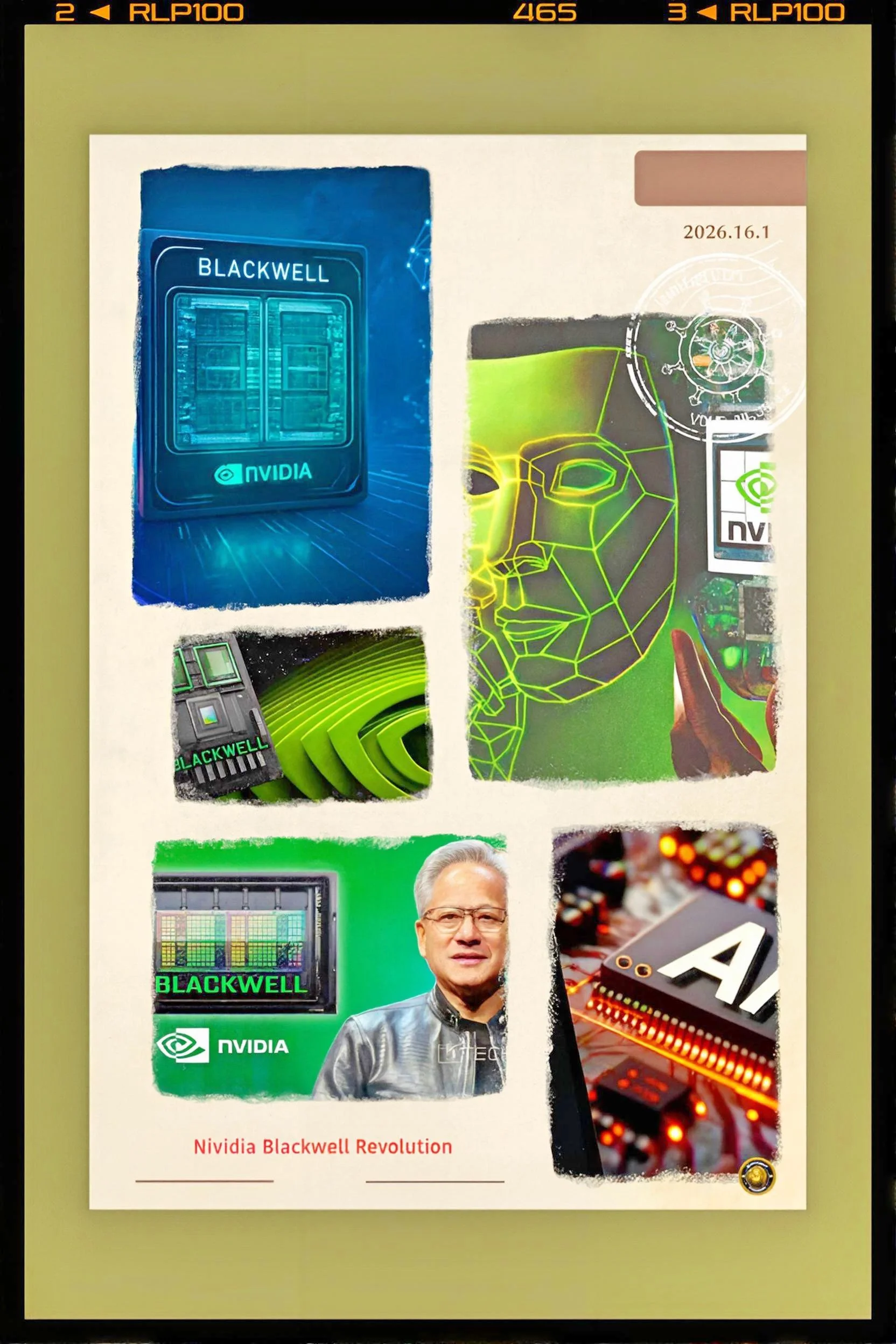
Blackwell, deployed beginning in 2024, introduced significant refinements: the second-generation Transformer Engine now supported FP4 precision arithmetic, doubling throughput relative to FP8 operations while maintaining acceptable accuracy through post-training quantization techniques.
These incremental advances accumulated into a dominant market position: by late 2025, Nvidia controlled approximately ninety-two percent of the discrete GPU market, with data center accelerators representing the highest-margin segment of the company's business.
Yet beneath this apparent dominance lurked a fundamental architectural constraint that even Nvidia's engineering prowess could not indefinitely overcome.
As AI models scaled in parameter count and as inference workloads proliferated across data centers, the bottleneck shifted. Compute performance, measured in floating-point operations per second, had advanced at exponential rates.
Memory bandwidth—the rate at which data could be transferred between the GPU's high-bandwidth memory and its computation cores—had advanced more slowly. This "memory wall," familiar to computer architects for decades but newly acute for AI workloads, emerged as the fundamental limiter of further performance scaling.
By 2025, leading researchers at companies including Nvidia itself acknowledged that memory bandwidth constraints represented the primary obstacle to reducing inference cost per token, a critical metric as inference became increasingly central to AI system economics.
Current Status
The Roadmap Through 2028: From Rubin's Power to Feynman's Revolution
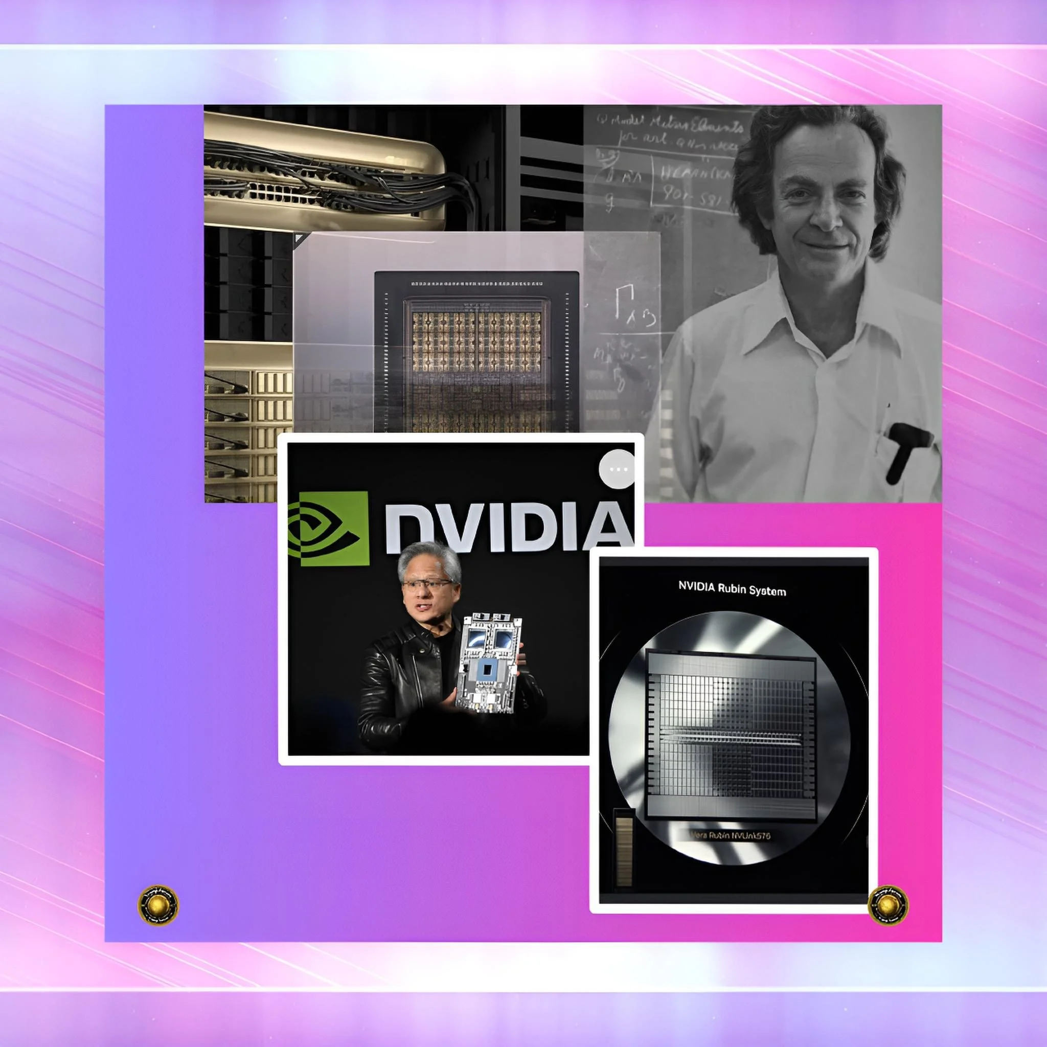
Nvidia's most recent strategic disclosure, articulated by CEO Jensen Huang at GTC 2025 and updated at CES 2026, provides unprecedented transparency regarding the company's technological vision through 2028.
The roadmap encompasses three generations of architectures spanning from Blackwell (2024-2025) through Rubin (2026-2027) and culminating in Feynman (2028).
More significantly, it reveals Nvidia's commitment to an annual release cadence coupled with synchronized evolution of CPUs, networking infrastructure, and interconnect technology. This holistic systems approach reflects a mature understanding that GPU performance alone no longer constitutes the primary constraint on AI system capabilities.
Rubin, scheduled for release in the second half of 2026, will introduce the Vera CPU—an eighty-eight-core custom ARM processor delivering twice the performance of the previous Grace processor while consuming only fifty watts. The Vera CPU will connect to Rubin GPUs via a 1.8 terabyte-per-second NVLink interface, enabling CPU-GPU integration that Nvidia claims delivers one-hundred-fold performance increases while multiplying power consumption by only three.
Rubin itself will achieve fifty petaflops of FP4 inference performance, more than double the twenty petaflops of Blackwell. In an NVL144 rack configuration, Rubin will deliver three-point-six exaflops of FP4 inference compute—three-point-three times greater than Blackwell Ultra's 1.1 exaflops.
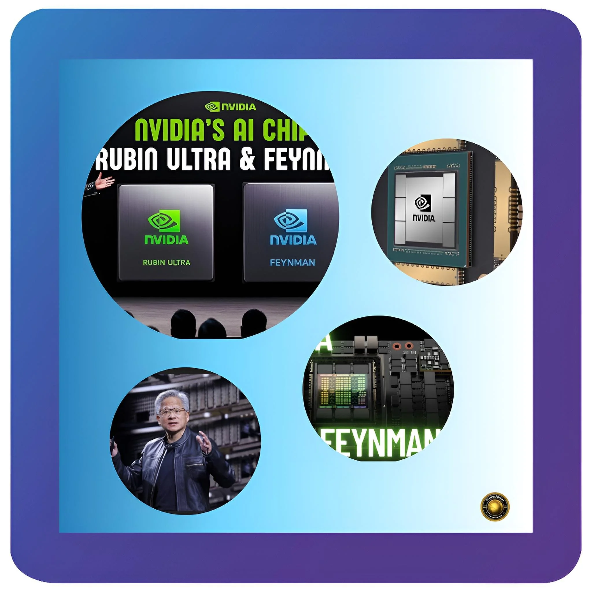
Rubin Ultra, arriving in the second half of 2027, represents a more substantial architectural advancement. Individual GPUs will comprise four reticle-limited dies, each capable of one-hundred petaflops of FP4 performance.
In a full rack configuration using 576 GPU chiplets across an NVL576 rack, Rubin Ultra will achieve fifteen exaflops of FP4 inference compute and five exaflops of FP8 training performance—roughly fourteen times more powerful than current NVL72 platforms based on Blackwell. Each GPU will integrate one terabyte of HBM4E memory, contributing to 365 terabytes of high-speed memory per complete rack. These figures are difficult to contextualize: a single NVL576 rack will deliver more inference compute capacity than existed in the entirety of the global GPU market a decade prior.
Feynman, the final architecture in this roadmap, represents an even more profound transformation. Scheduled for production in 2028 and utilizing TSMC's A16 process node, Feynman will constitute the first AI application to lead TSMC's most advanced process technology adoption, a historic reversal of the pattern whereby consumer electronics—particularly Apple's iPhone chips—first deployed each new TSMC generation.
The A16 node represents a significant engineering achievement: the 1.6-nanometer-class technology integrates gate-all-around nanosheet transistors with backside power delivery, an architecture that shifts power supply rails from the front surface of the wafer to the rear. This seemingly technical detail carries profound implications for large AI accelerators.
Key Developments
Architectural Innovation and Strategic Positioning: Why Backside Power Delivery Changes Everything
The decision to adopt backside power delivery for Feynman reflects a maturation of understanding regarding the physical constraints limiting AI accelerator scaling.
Conventional process nodes route both power and signal information across the front surface of a chip. As chips expand in size and power density increases, this creates iron fences around available area for signal routing. Congestion on signal interconnects delays propagation, increasing latency and power consumption. By migrating power delivery to the backside, Feynman frees an additional layer of front-side metal routing, providing approximately ten percent increased signal routing density and reducing voltage drop through shorter, lower-resistance power paths.
For Feynman specifically, this architectural freedom enables what industry analysts have termed "the Pouladian Cheat Code"—the practical integration of three-dimensionally stacked on-die SRAM through hybrid bonding techniques. Contemporary GPU designs incorporate primarily external high-bandwidth memory in the form of HBM stacks mounted through micro-bumps on the package substrate. This architecture provides enormous capacity but at the cost of finite bandwidth and significant latency.
Stacking SRAM directly atop the compute cores through hybrid bonding creates a memory hierarchy analogous to traditional CPU cache structures, enabling near-instantaneous access to frequently-used data while reducing the bandwidth demands on external HBM. The memory wall—the fundamental constraint limiting inference cost reduction—becomes passable through architectural innovation rather than brute-force bandwidth multiplication.
Feynman's adoption of the A16 process node represents a strategic decision of unusual boldness. Nvidia historically has deployed mature process nodes for its largest products, preferring yield stability and thermal characteristics over leading-edge process advantages. Hopper utilized TSMC's 4-nanometer node, which was two generations old by Hopper's introduction. Blackwell employed an even more conservative approach with TSMC's 4-nanometer-plus process.
This conservative positioning reflected fundamental physics: larger dies suffer worse yields and thermal challenges on early-generation process nodes. The decision to adopt A16 for Feynman suggests that Nvidia's engineering confidence in managing these challenges has grown substantially, or that competitive pressure from AMD and other rivals has necessitated earlier adoption of advanced nodes.
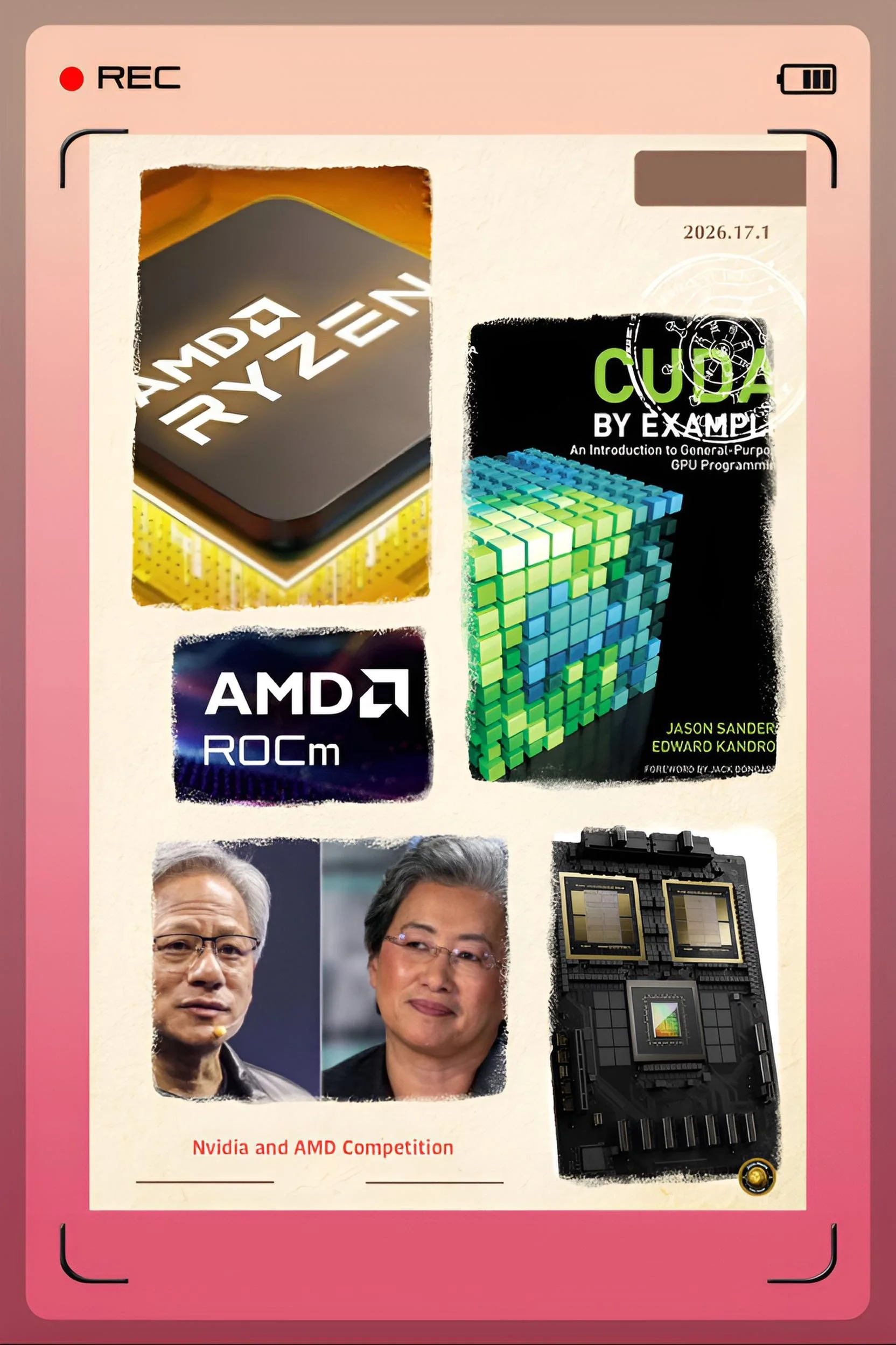
AMD's positioning provides crucial context for this decision. The company's MI350 and MI355X accelerators, announced in 2025, deliver impressive inference performance coupled with superior token-per-dollar efficiency compared to Nvidia's B200.
AMD has explicitly positioned inference as its primary competitive battleground, ceding the training market to Nvidia while attempting to carve out dominance in the expanding inference market. This strategy reflects economic realism: inference represents a substantially larger and faster-growing market than training, with enterprises seeking to deploy already-trained models across vast numbers of inference servers.
By 2030, AI inference market size is projected to exceed $250 billion, substantially larger than the training market projected to expand from roughly fifty percent of the total AI chip market.
Nvidia's Feynman response to this competitive challenge operates on multiple levels simultaneously.
First, by adopting the A16 process node, Feynman gains a full process generation advantage over AMD's anticipated MI400 architecture, likely to deploy on standard 2-nanometer nodes or earlier variants.
This process advantage, combined with backside power delivery optimization, could provide Nvidia with a performance-per-watt superiority that effectively ends competitive inference challenges for several years.
Second, the focus on inference optimization through memory hierarchy restructuring rather than compute multiplication reflects recognition that inference challenges differ fundamentally from training challenges.
Training demands maximum parallel computation; inference demands low-latency, memory-efficient data movement.
Latest Facts and Concerns
Supply Chain, Power Consumption, and Adoption Challenges: The Infrastructure Bottleneck
The realization of the Feynman vision depends critically upon several contingencies, some within Nvidia's control and others determined by external factors.
TSMC's A16 process requires mass production beginning in the second half of 2026. Historical patterns suggest that first-customer products utilizing new process nodes appear twelve to eighteen months following mass production initiation, placing Feynman's earliest production in late 2027 or early 2028.
The process node costs approximately thirty thousand dollars per wafer—among the highest in the semiconductor industry, reflecting the extraordinary complexity of implementing both gate-all-around transistors and backside power delivery simultaneously.
For Feynman GPUs, cost-per-unit will substantially exceed current Blackwell pricing, likely positioned between thirty thousand and forty thousand dollars per unit. This pricing, combined with limited initial supply, suggests that Feynman deployment will initially concentrate among hyperscalers with enormous inference requirements rather than diffusing broadly across the industry.
Power consumption emerges as an equally significant concern. Rubin GPUs consume 1,800 watts each. Rubin Ultra GPUs, despite moderate frequency increases relative to Rubin, will consume higher absolute power due to increased chiplet count and density.
Feynman specifications remain undisclosed, but industry analysts project that a full NVL576 Feynman rack could exceed 1.2 megawatts, requiring data centers specifically engineered for extreme power density. This escalation occurs amid a broader infrastructure crisis: the United States is projected to require between fifty and one-hundred-thirty-two gigawatts of data center power by 2028, with AI-specific infrastructure consuming between twenty and twenty-five gigawatts.
Current data center construction rates and electrical grid expansion timelines appear insufficient to accommodate this demand. Permitting delays, transmission bottlenecks, and renewable energy infrastructure limitations create a fundamental constraint on AI infrastructure deployment that no amount of architectural innovation can overcome.
Water consumption presents a parallel constraint. Hyperscale AI data centers currently under construction are projected to consume sixteen to thirty-three billion gallons of water annually by 2028, primarily for cooling.
Several regions crucial to data center development—particularly the southwestern United States—face severe water constraints. Some hyperscalers have begun implementing direct liquid cooling and closed-loop systems to reduce consumption, yet these techniques add considerable engineering complexity and capital cost.
The memory supply chain presents additional constraints. Feynman will depend upon HBM5 memory—the fifth generation of high-bandwidth memory technology. Samsung, SK Hynix, and Micron are racing to qualify HBM5 production, but yields remain uncertain and capacity constraints are nearly inevitable.
Even HBM4E, deployed beginning with Rubin, shows signs of supply constraints. The tight coupling between GPU availability and HBM supply means that any bottleneck in memory production directly constrains system availability.
Cause and Effect Analysis
The Path to Feynman as Solution to the Inference Cost Crisis: From Crisis to Optimization
The trajectory toward Feynman reflects a specific causal chain beginning with the economics of AI inference deployment. When OpenAI's GPT-4 was released in 2023, inference at scale proved economically unviable for most applications.
The cost of processing a million tokens through the model exceeded sixty dollars, placing real-time inference beyond the reach of applications requiring responsive behavior. This inference cost crisis motivated an industry-wide search for optimization techniques.
Initial approaches focused on model optimization: quantization reduced model precision from FP32 to FP16, FP8, or even FP4, maintaining acceptable accuracy while reducing memory and compute requirements by factors of two to sixteen. Knowledge distillation, speculative decoding, and pruning provided further marginal improvements.
Yet these techniques operated within the constraints of existing hardware architectures. At some point, further software optimization reaches diminishing returns: even with perfect algorithmic optimization, the fundamental bottleneck of external HBM bandwidth limits throughput. This realization drove the search for architectural innovations.
Nvidia's response crystallized around three concrete solutions: the adoption of lower-precision arithmetic natively supported in hardware rather than through software emulation; the implementation of memory hierarchy innovations through hybrid bonding and three-dimensional stacking; and the integration of more capable CPUs to handle sequential reasoning tasks that GPUs process inefficiently.
Feynman consolidates these solutions.
The architecture's support for native FP4 and other ultra-low-precision formats, combined with post-training quantization and quantization-aware training techniques, enables accuracy-preserving inference at one-quarter to one-eighth the memory bandwidth of conventional high-precision approaches.
The three-dimensionally stacked SRAM, enabled by backside power delivery and hybrid bonding, provides nanosecond-latency access to frequently-accessed data without drawing from off-package HBM.
The Vera CPU handles sequential reasoning workloads—tasks inherently ill-suited to GPU parallelism—while the GPU focuses on the matrix multiplications endemic to transformer inference. The combined effect is projected to reduce inference cost per token by factors approaching one-hundred relative to current systems while simultaneously decreasing power consumption and enabling deployment of trillion-parameter models on single-rack systems.
Future Steps
Adoption Timeline, Ecosystem Maturation, and Competitive Dynamics: What Comes After 2028
The path from Feynman's anticipated 2028 release to widespread deployment encompasses several crucial phases.
The first phase, anticipated to span mid-2027 through mid-2028, will involve engineering samples provided to the largest hyperscalers—likely Google, Amazon, Microsoft, and Meta.
These customers will integrate Feynman into their data center designs and conduct performance validation. During this phase, Nvidia's software teams will mature the CUDA ecosystem, ensuring that popular frameworks, inference serving systems, and model optimization tools support Feynman's novel architectures. The TensorRT-LLM inference server, Nvidia's Model Optimizer, and CUDA libraries will be hardened for Feynman's three-dimensional memory hierarchy and ultra-low-precision arithmetic.
The second phase, spanning 2028 through early 2029, will see initial volume production and deployment. Hyperscalers will begin installing Feynman-based systems in production data centers, initially in limited configurations to validate designs and operational procedures.
This phase will likely see Feynman priced at a significant premium to contemporary Blackwell or Rubin systems, with only the largest organizations deploying the architecture. Error rates and reliability issues will emerge and be iteratively resolved.
The third phase, spanning 2029 and beyond, will see broader adoption as supply increases and early production issues are resolved. The question of whether a single-chip next-generation architecture follows Feynman or whether Nvidia continues the Feynman line with incremental updates (Feynman Ultra, for instance) remains undisclosed, but historical patterns suggest continuation through 2030 at minimum.
Nvidia's primary competitive challenge during this period will come from AMD, whose MI400 architecture, likely deploying on standard 2-nanometer nodes without backside power delivery, could achieve competitive performance per watt with substantially lower cost per unit.
If AMD successfully captures a meaningful share of the inference acceleration market, Nvidia's margins would compress and competitive dynamics would intensify. However, Nvidia's historical software ecosystem advantages, particularly the maturity and performance of the CUDA toolkit, create substantial switching costs that favor incumbent dominance.
A customer deploying Nvidia infrastructure in 2028 will have made software investments in CUDA, TensorRT, and Nvidia-specific optimization techniques that create path dependency. Switching to AMD would require software rewrites, compatibility testing, and potential performance compromises. These switching costs likely ensure Nvidia's continued dominance even if AMD achieves hardware parity.
Custom silicon presents a more distant competitive threat. Google's TPU, Amazon's Trainium, and Cerebras' custom architectures all faced pressure as Nvidia's generalist accelerators became increasingly capable and cost-competitive.
Feynman's advances in inference efficiency could accelerate the trend away from custom silicon toward Nvidia GPUs, reducing the incentive for hyperscalers to invest in separate silicon development. Only for internally-deployed models with highly specialized inference patterns would custom silicon remain competitive.
Conclusion
Implications for the AI Compute Landscape Through 2030: The Limits of Silicon Engineering
The Feynman architecture represents more than an incremental GPU advance. It signals Nvidia's commitment to sustaining technological leadership across the AI compute spectrum through architectural innovation rather than brute-force scaling.
The company's decision to adopt leading-edge TSMC process technology ahead of Apple, to integrate novel memory hierarchies through three-dimensional hybrid bonding, and to couple specialized CPUs with GPUs reflects a matured engineering vision aligned with genuine market requirements rather than theoretical performance metrics.
The broader implications extend across multiple dimensions. For the semiconductor industry, Feynman validates the thesis that AI workloads justify early adoption of advanced process nodes, potentially shifting the innovation cycle such that AI applications, not consumer electronics, drive technology roadmaps. For data center operators, Feynman promises dramatic cost reductions in inference deployment, enabling classes of applications previously economically infeasible.
For competitive dynamics, Feynman likely extends Nvidia's dominance through at least 2030, after which further architectural innovations will determine whether the company maintains its position or faces genuine competitive disruption.
The one uncertainty that Feynman cannot resolve involves infrastructure constraints.
Even the most efficient AI inference chips cannot overcome grid transmission bottlenecks, water scarcity, or permitting delays.
The bottleneck limiting AI deployment by 2028 will not be compute capability but rather power supply, cooling capability, and site availability.
Nvidia's engineers can create chips of extraordinary capability, but they cannot engineer the electrical grid or reshape the geography of water availability.
For this reason, the practical impact of Feynman on the AI landscape will depend as much on infrastructure policy decisions as on architectural innovations.
The company that produces the world's most advanced inference chips cannot deploy them at scale without power. For the first time in modern technology history, the constraint on AI deployment may lie entirely outside the purview of silicon engineering.